This thread has been locked.

If you have a related question, please click the "Ask a related question" button in the top right corner. The newly created question will be automatically linked to this question.

UC1825B-SP: UC1825 - Output PWM stability (open loop)

Part Number: UC1825B-SP
Other Parts Discussed in Thread: UC1825

Hello,

Due to instabilitty on PUSH PULL converter base on UC1825B, we investigate on the EA of the PWM driver.

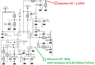
We tested without power stage, with the following setup :

  - EA of UC1825 is mounted in non inverter mode.

  - we injected a very clean DC voltage (red figure on the schematic)

  - we measured with oscilloscope variations on the duty cycle around 0.8% (60ns on the period : 7.87us)

  - We respected max sink and source current of EAout.

  - Output PWM can reach full range of 0-95% of the DC.

Do you have any information on this problem?

We have high voltage on the output. So the transformer have high gain, and the regulation loop is slow. So little variation on the Duty cycle cause high variation on the output voltage....

All of our power supply are clean.

We tested to add capcitor on C17, 10nF solve a part of the problem, but kill the bandwith of the loop.

Other information : If we haven't injection voltage, the PWM is in full Duty cycle (95%), because EA is in saturation mode, so in this case the output PWM is very stable, there is no variation.

Thanks for your support

  • Hey Vincent,

    The controller creates the duty cycle based on a triangle wave through the RAMP pin.
    You can try creating your own triangle waveform in the RAMP pin in order to create less variation in the output duty cycle.

    Thanks,
    Daniel

  • Hello Daniel,

    I minotored the RAMP and the OSC, but there is no variations on they signals.

    Have ever meet this jind of problem? Do you consider, this is a normal operation?

    About your proposal, if I do this with a Waveform generator, how can I synchronise the RAMP on the OSC?

    Thanks

  • Hey Vincent,

    You can sync your device to the waveform generator by creating a spike on the CT pin. This is shown in the datasheet on page 10.
    A variation of 60 ns seems like normal operation at first glance.
    I am giving suggestions on how to figure out where this variation is coming from
    0.8% variation could me just mV of change in the signals internally.

    I know that your application requires tight voltage control, but that is generally done when is closed loop.
    While the duty cycle will vary a bit, this should be corrected by the loop over time.

    Thanks,
    Daniel