This thread has been locked.

If you have a related question, please click the "Ask a related question" button in the top right corner. The newly created question will be automatically linked to this question.

TPS543C20: Capability of handling high transient current

Part Number: TPS543C20
Other Parts Discussed in Thread: LM10011, INA226

Dear TI Team,

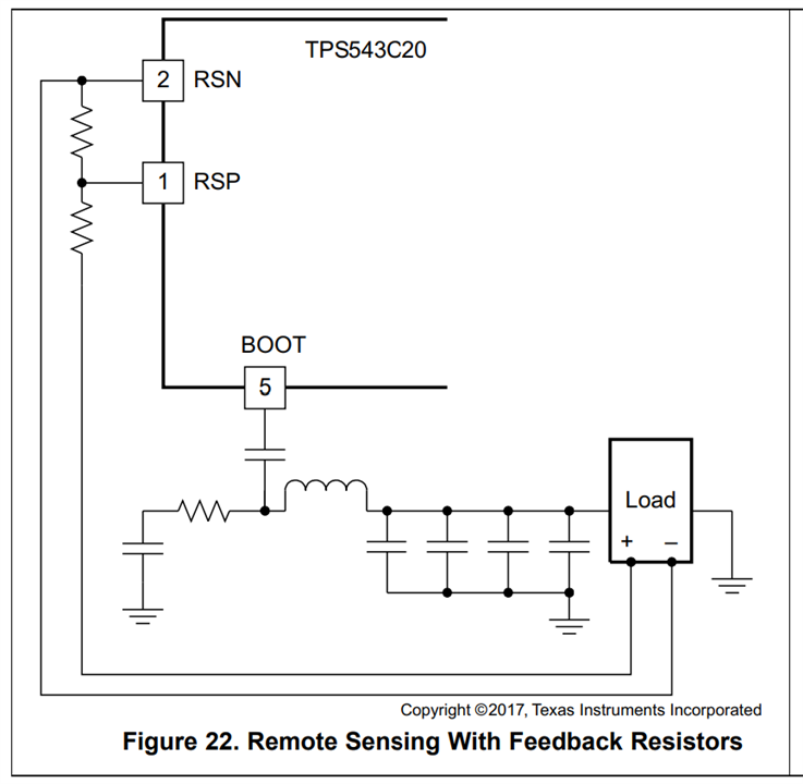
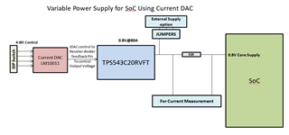
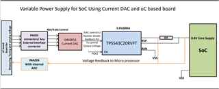
We are using  TPS543C20RVFT ( 2 Phase stacked Configuration for 80A ) IC in our design. This is used for supplying 0.8V core supply of our major SoC chipset. During PI transient simulation we found that the chipset may produce 130-140A high current transients in the duration of 1ns - 10ns.

1. In this case whether IC will be able to handle such high transients.?

2. What is maximum transient that the IC can handle ( 2 Phase stacked configuration ) ?. As per one of our earlier discussion its been told that 120A can be handled by stacked 2-Phase configuration ( 60A each ). In this case what is the maximum pulse width/the transient time with 120A that IC can withstand.

3. If TPS543C20RVFT IC is unable to handle such high transient currents, then what will happen for the IC if such high transient is been introduced by load. Will it go to over current protection state and blank out or IC will go bad. 

4. How much minimum decoupling capacitance should be provided on the board to handle such high surge currents in VRM. Please provide your input for the same.

Best Regards,

Vyshnav Krishnan  

  •  

    The TPS543C20's current limit and current handling capabilities are limited by its switches and current limit functions.  A load current pulse of 1-10ns will be handled by the output capacitors and will not propagate back through the inductor to the TPS543C20's power FETs.  Supporting load current transients on time scales less than a few microseconds depends entirely on the ESR and ESL of the output capacitors and their PCB layout.  The converter and inductor will support these very fast load transients averaged over the time constant of the converter's closed loop bandwidth.

    1. In this case whether IC will be able to handle such high transients.?

    The TPS543C20 includes a 60A (typical) high-side FET current limit which will truncate the switch current with a peak of 60A, delivering a maximum inductor current less than 60A to the output capacitors.  Load currents greater than this high-side FET current limit will be handled by the output capacitors, decreasing VOUT.  In addition, the TPS543C20 implements a low-side current limit.  The low-side current limit extends the off-time, limiting the valley current of the inductor.  This can limit the output current to less than 60A depending on the ILIM setting

    If VOUT drops below the Power Good lower threshold (falling), PGOOD will assert low.

    If VOUT drops below the Under Voltage Protection threshold (falling) the converter will shut-down, time out, and then restart (Hiccup)

    2. What is maximum transient that the IC can handle ( 2 Phase stacked configuration ) ?. As per one of our earlier discussion its been told that 120A can be handled by stacked 2-Phase configuration ( 60A each ). In this case what is the maximum pulse width/the transient time with 120A that IC can withstand.

    The converter can sustain 60A load current for an extended period of time, but operation in circuit will depend on the value of Cout and how far above the current limit the transient current is, as excess current will decrease VOUT and trigger Under Voltage Protection.

    3. If TPS543C20RVFT IC is unable to handle such high transient currents, then what will happen for the IC if such high transient is been introduced by load. Will it go to over current protection state and blank out or IC will go bad. 

    The High-side and Low-side current limits will clap the switch current, leaving the output capacitors to deliver the differential current until Under Voltage Protection triggers a shutdown.

    4. How much minimum decoupling capacitance should be provided on the board to handle such high surge currents in VRM. Please provide your input for the same.

    A 10ns pulse at 150A contains 1.5μC of charge.  The amount of output decoupling capacitance needed to support such a transient depends on the output voltage deflection needed to maintain during that 10ns.  Due to the high dI/dt, that output capacitance will likely need to be made with a large number of small ceramic bypass capacitors very close to the loading IC, and will depend on the voltage deflection allowed.  150μF with virtually no ESR or ESL due to being made from a large number of smaller capacitors, would discharge 10mV during that 10ns.

    Additional larger ceramic capacitors and bulk capacitors will likely be needed to support the average transient to the bandwidth of the converter as well, but the amount needed depends heavily on the Switching Frequency, Inductor Value, and the change in time-averaged load current.

    1) What is the minimum time-averaged loading current seen by the converter averaged over 3 switching cycles?

    2) What is the maximum time-averaged loading current seen by the converter averaged over 3 switching cycles?

    3) What is the allowed output voltage deflection (change in Vout) in response to the transition between these two states?

    4) The peak output impedance of the converter must be equal to or less than ΔVout / ΔIout

    5) The output capacitors will need to provide that output impedance, or less, at the closed loop bandwidth of the converter.  For switching frequencies up to 500kHz, 1/5 the switching frequency is generally obtainable.  For switching frequencies above 500kHz, the bandwidth beyond 100kHz is typically reduced by about 2kHz for each 100kHz past 500kHz due to additional loop parasitics above 100kHz.  (@ fsw = 600kHz, 118kHz bandwidth, @ 700kHz, 134kHz bandwidth, etc)  These are estimates of the approximate bandwidth that will be achievable for sizing output capacitance.  Layout and component selection can affect the loop capabilities.

    To calculate the output impedance of a capacitor at a given frequency, use the formula ESR + 1/ (2*pi*f*C) for each capacitor and then consider Zout of all of the capacitors in parallel.  Zout(total) = 1 / ( 1/Zout1 + 1/Zout2 + 1 / Zout3...)

  • Dear Peter,

    Thank you so much for the quick response and detailed explanation. 

    So how much ever transients come beyond 60A should be handled by on-board capacitors and PDN right.?

    I have one more question regarding same part. But this is completely different from our earlier discussion.

    Currently we are setting the output voltage by mounting resister to VSEL Pin of the power regulator ( dual phase stacked).

    We are designing a characterization for the same SoC and we wanted to vary the core voltage by +/-15% (Core voltage is 0.8V).

    So we are planning to use a current DAC with P/N: LM10011. 

    1. In case of current DAC, we should connect DAC current output to the feedback pin of regulator and it will change the feedback voltage, which in turn change the output voltage. So in case of TPS543C20RVFT IC connecting DAC current output to VSEL pin will help to vary the output voltage or not.?

    2. If not is there any solution to vary the output voltage of regulator using a DAC.? 

    Kindly provide your valuable input to proceed further.

    Best Regards,

    Vyshnav Krishnan

  •  

    In the future, when asking a new question not related to the original question and thread title, please create a new question.  That helps other engineers search for and find the answers to the questions more easily.

    However:

    Yes, the TPS543C20 can work with the LM10011 current DAC to provide parallel VID for dynamic voltage change, static voltage scaling, or margin testing.

    Since the LM10011 can only source current, no sink capability, you will need to see up the TPS543C20 to generate the highest desired output voltage when the LM10011 is sourcing no current and the lowest desired voltage when the LM10011 is sourcing the most current.

    For 0.8V +/- 15% (0.68V - 0.92V) Leave the VSEL selection at 0.8V and add an external divider between VOUT, RSP and RSN to raise VOUT to 0.92V when the LM10011 is not sourcing the lowest amount of current.

    Size the top resistor (VOUT to RSP) for 120mV of drop with the DAC current difference between the MSB (Code 1000) and MSB -1 (Code 0100) of the DAC is enabled (15μA)  (120mV / 15μA = 8kΩ.  The closest standard resistor is 8.06kΩ

    Size the bottom resistor for 0.92V when VRSP = Vref = 0.8V and IDAC = MSB = 1 (Code 1000, 26.4μA)

    (Rbot = Vref / [ ((Vout - Vfb) / Rtop + Idac @ 1000 ] = 0.8V / [ (0.92V - 0.8V) / 8.06kΩ - 26.4μA ] = 0.8V / (14.88μA + 26.4μA) = 19.38kΩ

    Closest standard value is 19.1kΩ

    Set LM10011 to 4-bit mode by pulling the MODE pin to VDD

    To select 0.92V, Release Bit 3 only (VIDS = 1, Code 1000)

    To select 0.8V, release Bit 2 only (VIDC = 1, Code 0100)

    To select 0.68V, hold all VID pins low (Code 0000) 

    The LSB adjustment resolution of the 4-bit DAC is 30mV.

    This provides simple, single bit VID transitions between 0.68V, 0.8V, and 0.92V for margining, but does not make full use of the resolution capabilities of the LM10011.  If you need better resolution between 0.68V and 0.92V, we can adjust the resistor values to make use of the full scale capabilities of the LM10011. 

  • Dear Peter,

    As this regulator doesn't have external voltage divider option and voltage is set by using a single resister connecting to VSEL pin, can we connect divider circuitry to VSEL pin in such a way that feedback voltage will be sourced to VSEL pin.?

    Could you please clarify  "Leave the VSEL selection at 0.8V and add an external divider to raise VOUT to 0.92V when the LM10011 is not sourcing current."

    As there is no specific FB pin is available, how this voltage divider circuit to be connected.

    Kindly provide your valuable response.

    Thanks & Regards,

    Vyshnav Krishnan

  •   

    My apologies for using the incorrect pin label.  That should be the RSP pin not the FB pin.

    The TPS543C20 can be used with a resistor divider to select a voltage other than the reference listed in table 8.4.4 using the circuit described in Figure 22, Section 8.4.16.

    Rtop is placed between Vout and RSP and Rbot is placed between RSP and RSN.

    The LM10011 current is then sourced into the RSP node.

    I will edit the prior response to correct the FB / RSP pin label.  Again, my apologies for that.

  • If your layout does not allow for a resistor divider between VOUT, RSP and RSN, but already includes the LM10011 injection into the RSP net, that too can be worked, as long as there is a location in the layout for a resistor from VOUT to RSP, by changing VSEL to a resistor value greater than 0.92V, but that will require more complex VID selections to achieve 0.92V, 0.8V and 0.68V.

    The design is much simpler with the RSP to RSN resistor.

  • Hi Peter,

    Thank you for the input. We are designing a fresh version of board so we can take care this in design. So in this case, We can provide voltage divider in RSP and RSN pins. But how VSEL pin should be treated.? can we keep it floating or we should connect corresponding resister value for 0.8V to VSEL pin.? 

    Also what will be the feedback voltage when we use RSP and RSN pins for voltage divider. 

    Please find the attached reference image of the implementation.

    Thanks & Regards,

    Vyshnav Krishnan

  •  

    The TPS543C20 regulates the output voltage by driving the RSP - RSN = VREF, where VREF is set by the VSEL resistor.

    When there is no resistor between VOUT and RSP and no resistor from RSP to RSN, then RSP will be equal to VOUT, and VOUT will be regulated to the VREF voltage selected by the VSEL resistor.

    When there is a resistor between VOUT and RSP and a resistor from RSP to RSN, the TPS543C20 will continue to regulated the voltage at the RSP pin equal to the reference voltage selected by the VSEL resistor, but the output voltage will be a scaled version of that voltage.

    For example, if the VOUT to RSP resistor = RSP to RSN resistor, the RSP voltage will be 1/2 the VOUT voltage and VOUT will be regulated to 2x VREF when RSP = VREF.

    My above calculations are based on VREF = 0.8V, so:

    VSEL still needs to be terminated to GND to select VREF = 0.8V (23.7kΩ to GND)  Floating the VSEL pin would result in VREF = 1.0V, which would require a different resistor divider and different VID codes to select the desired 0.68V, 0.8V, and 0.92V options.

    The RSP voltage will be 0.8V

  • Hi Peter,

    Thank you for the explanation. I have few queries regarding how this can taken care in dual phase stacked configuration.

    1. VSEL resister should be connected to both master and slave devices or not.?

    2. Feedback resister should be provided using RSP and RSN for both master and slave devices or not.?

    Kindly provide input for above queries as well.

    Best Regards,

    Vyshnav Krishnan

  • Hi Vyshnav,

    Peter will check it tomorrow. Thanks.

  •  

    Refer to the reference schematic for a two-phase application section 9.3.1 - Figure 32

    RSP and RSN are only connected to VOUT for the primary device (master) of the stack.

    VSEL is terminated with a resistor on only the primary device.

    The secondary device does not need VSEL programming since it's voltage loop is bypassed and the current control loop is run by the primary device.

    VSEL, RSP, and RSN can be shorted to ground.

  • Dear Peter,

    Thank you for the input. We are planning to vary the voltage in steps of 20mV and we hope TPS543C20 will be able to support this variation in voltage. We will make sure that closed loop path will be there to compensate output voltage.

    We may need your help to review the schematics, once its done. 

    Thanks & Regards,

    Vyshnav Krishnan

  •  

    For 20mV resolution, you will need to select different resistors than the ones I posted above, but 20mV steps are within the resolution of the LM10011 using the TPS543C20, though the codes to select 0.68, 0.80 and 0.92 will be a little more complicated.

    For 20mV resolution with the 3.76μA LSB of the LM10011, you'll want a top resistor of 5.36kΩ

    You can then size the bottom resistor to select 0.8V at mid-scale (1000) to allow 140mV up positive adjustment and 160mV of negative adjustment.

    Code 8 (RSET = 140kΩ) has a current of 26.4μA.  To set VOUT = 0.8V with a 0.8V reference, the bottom resistor will need to be 30.1kΩ.

  • Dear Peter,

    We are in design stage of this characterization board and we came across with one doubt.

    As per the LM10011 datasheet, they are considering full voltage range sweep to vary the voltage and maximum voltage will be set for 0 current value.

    In case of 0.8V output voltage, 0.92V will be set for 0 current value and startup voltage will be 0.8V. In this case the resister value calculation is entirely different from than you mentioned above. Could you please help me in understanding how the VID value is selected as per above calculation.?

    Best regards,

    Vyshnav Krishnan 

  • You said that you wanted to cover the range of 0.68 to 0.92 with a nominal value of 0.80V and a step of 20mV.  Rather than set the 0A (Code b'1111) value to 0.92V, I set the mid-scale (Code b'1000) to 0.8V.  That allows for a range of 0.62V to 0.94V.  If you set 0.92V at the current current level, with 20mV steps, the adjustable range would be 0.60V to 0.92V.  It's really where you want to set the extra 60mV of adjustable, whether you want to split it between positive and negative, or you want to bias it to one side or the other.  If you want to set the range for 0.60V to 0.92V, size the resistor divider for 0.8V when CODE b'1001 is selected (Rset = 154kΩ, Idac = 22.6μA, which calculates to 35.4kΩ, the closest standard value being 35.7kΩ)

    You want to set the divider based on the target nominal voltage, not one of the end points because it's the nominal voltage you want to be most accurate.

  • Dear Peter,

    Please find the attached image shows the implementation we are planning for TPS543C20 Regulator. Below are our concerns

    1. Regulator output at load side is connected to sense pins of it, so even if some voltage drop is happening the output voltage will be compensated by the regulator. But we are planning to use INA226 ADC to measure the current, voltage and power. This data will be provided to a uC based board to adjust the output voltage according to the exact voltage value at the load. So regulator itself will be adjusting the voltage as well as the controller will try to vary output if drop is happening. This will lead a conflict that controller will adjust voltage even if regulator is adjusted by itself. Please correct me if am wrong. 

    So un this case how we can take care this.

    Thanks & Regards,

    Vyshnav Krishnan 

  •  

    The LM10011 will make adjustments to the regulation target of the TPS543C20, so the two loops wont be fighting, but the best option would be to set the sense point for the resistor divider to RSP to the point you want regulated.  The LM10011 will have 20mV resolution, so it's not going to be able to make fine output voltage to adjust to cancel small drops across the current sense resistor.

    With the top resistor of the RSP to RSN divider connected to Vout after the current sense resistor, the analog loop should cancel the drop across the current sense resistor.

  • Dear Peter,

    We have completed design using TPS543C20 in dual phase stacked configuration. The LM10011 current DAC is used in 6 bit mode to vary the output voltage in the range of 0.686V to 0.926V by keeping nominal value at 0.8V for 30.1uA current, RSET = 118K. An ADC with P/N INA226 is used to measure voltage, current and power at the load side. The DAC and ADC are connected to a controller board. The measured value from ADC will be checked by the controller board and the DAC current will be varied accordingly. Here remote sensing option is provided in case of both regulator as well as ADC. Please find the attached schematics section of the same. Request you to review the same and provide your feedback. Please let me know for any further clarifications.

    4111.TI TPS543C20.pdf

    Best Regards,

    Vyshnav Krishnan

  • Hello Vyshnav, 

    Peter is out of office coming back next week. 

    So I am filling up for him. 

    Can you please use the attached excel calculator tool and the check list with the your design requirements.   

    I can provide further inputs once that is done. 

    Thank You!

    Tahar

    slurb00.zip