This thread has been locked.

If you have a related question, please click the "Ask a related question" button in the top right corner. The newly created question will be automatically linked to this question.

UCC256404: LLC converter switching off and on again periodically

Part Number: UCC256404
Other Parts Discussed in Thread: UCC256402

Hi guys,

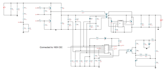
I am doing research towards efficiency in DC-DC converters. In this research, I'm designing a 160V-12V LLC converter for low powers (25W maximum) with the UCC256404 controller, I've added a screenshot of my circuit down bellow. My circuit is based on a WEbench generated design. The primary side of the transformer has 20 windings, auxiliary and both secondary windings have 3 windings. I'm monitoring some strange behavior: It seems like everything is switching on and off periodically.

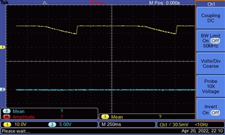
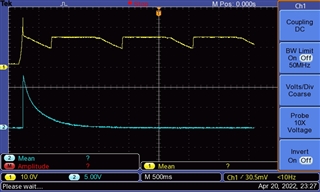
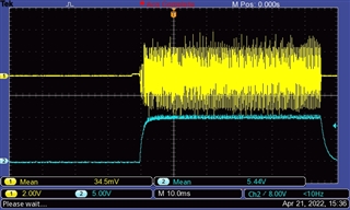
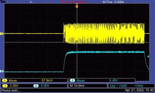
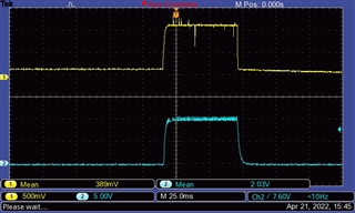
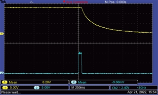
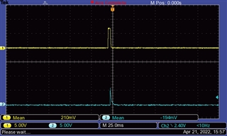
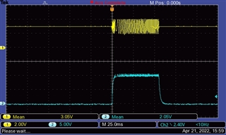
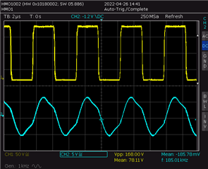
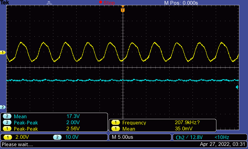
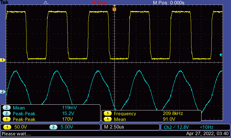
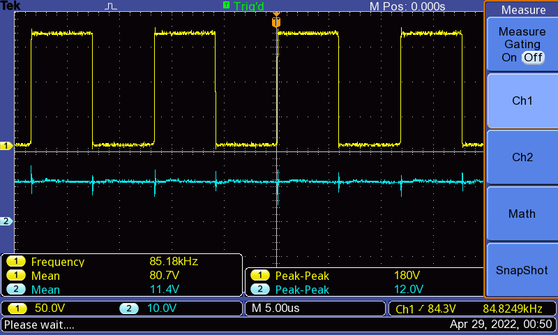
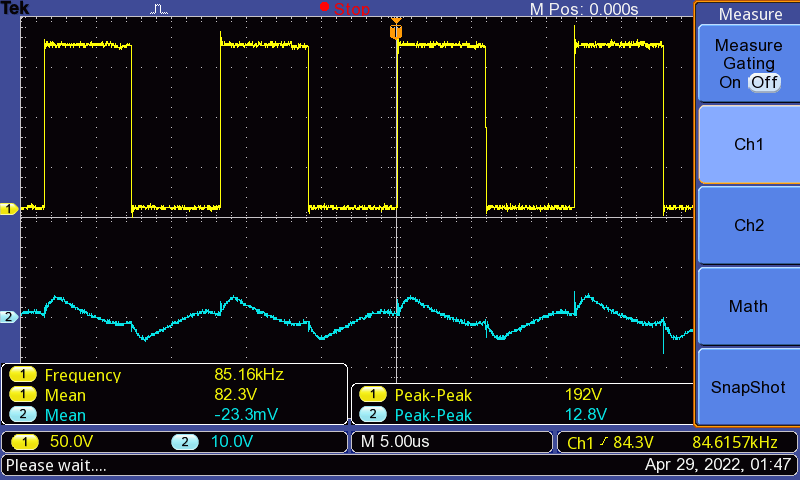
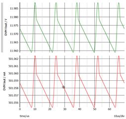
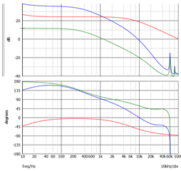
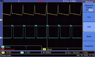
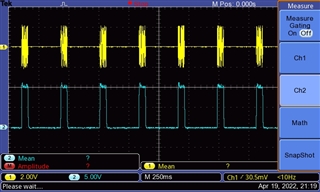
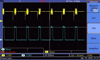
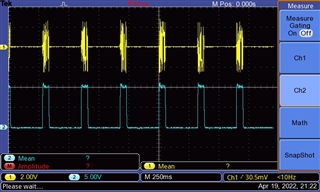
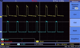
Bellow, I've attached some screenshots of measurements I did. Note the quite large time axis width: it seems like everything is on for 50 ms, and then off again for around 250 ms. In the 50 ms on period, I'm having quite 'normal' behavior with my MOSFET drivers (high frequency switching, I did not include a screenshot of this). I've already looked over the data sheet, and made some experimental changes. From this I can conclude that the controller does not enter fault state (since the off period is not taking 1s, which would be the case for fault state according to data sheet), and that it is not an issue of the controller going into burst mode (I've tried my circuit with Rbw1 = 11 k and Rbw2 = 3.4 k, which should put it into mode 7, which turns off the burst mode). It seems like I'm having some problems with my VCC, since I'm not able to keep it at a constant. I do however not have a clue from where this problem is comming.

First picture is my design, then there are screenshots of different pins with the measured output. Next to that, at the BLK pin, I measure a constant of around 1V (which is expected, since I just input a source voltage of 160V)

ch1: VCC, ch2: Vout


ch1: RVCC, ch2: Vout

ch1: ISNS, ch2: Vout

ch1: VCR, ch2: Vout

ch1: BW, ch2: Vout


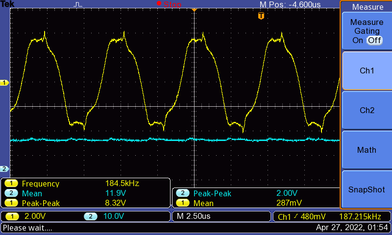
ch1: LL/SS , ch2: Vout

Regards,

Arne

  • Hi Arne,

    Thanks for reaching out to us.

    The HV pin of the UCC25640x should be connected to rectified AC through 5kohm as given in below schematics :

    PFCLLCSREVM-034 User Guide (ti.com)

    UCC25640EVM-020 User Guide (Rev. B) (ti.com)

    If the HV pin of 404 doesn't see any zero crossing, it is going to inject the xcap discharge current at HV pin which will heat up the IC and may hit over temperature limit.

    If there is no rectified AC is available, you can use UCC256402 where there is no xcap discharge feature. In this case you can directly charge the VCC through DC bus input voltage of the LLC. 

    Could you share the design calculator with me with the values used for your schematic.

    It would be easy for me to give suggestions if you share the design calculator (https://www.ti.com/lit/zip/sluc675 )

    Here is my observation from one of your waveforms:

    ch1: VCC, ch2: Vout

    Start up is initiated as soon as VCC charges to 26V. However, As soon as Converter starts switching, VCC voltage is getting reduced so fast. When the VCC hits VCCReStartJfet (9.65V), JFET turning on again to charge the VCC.

    Can you increase the VCC capacitance value see if that solves the issue?

    May I ask transformer construction details? How the auxiliary winding is wounded? Is it on primary or secondary winding? 

    Regards

    Manikanta P

  • Hello Manikanta,

    Thanks for your response. 

    regarding the X-cap discharge: is this a general remark of which I should be aware, or is there a possibility that this is the cause of the problem that I'm currently having? Unfortunately, the UCC256402 controllers are out of stock for all suppliers, even the TI website itself says 'out of stock'. Would it work,if I were to apply a small sine wave with a sine wave generator in my test setup? This would not be a permanent solution, but it would fix that problem in my test environment for now.

    This is my design calculation sheet. I wasn't sure what to fill in for the CR value at line 93, since my CR actually are two capacitors: one attached from GND to the lower part of the primary winding, and one from the lower part of the primary winding to the 160V input, both are 20 pF.

    8664.UCC25640x Design Calculator Rev4.0.xlsx

    Currently, I'm having 120 µF at VCC. My first thought would be that this should be plenty, but I will add some extra and repport the result to you ASAP! Also, the structure of my transformer is primary at the lowest layer (20), then a layer with both secondary windings (2x 3), then the auxiliary (3).

    Regards,

    Arne

  • Hello Manikanta,

    I think I've found the source of my problem: when I was measuring the auxiliary winding voltage, it only got as high as around 10V, which would make only around 9.5V after the diode, which is bellow the VCCReStartJFET. Therefor, I've added 2 windings to my auxiliary, making it 5 in total (aiming at 20V out of the auxiliary winding).

    However now I'm having a bigger problem: my controller is doing nothing at all: I've added the first screenshot of ch1=VCC and ch2=Vout. As you can see, VCC keeps on going periodically between around 15V and 10V (could be the 9.65V), Vout is doing nothing. I can confirm that VCC reaches the 26V at the start (second screenshot shows VCC on ch1 and RVCC at ch2 at the very start), but it only does this once. In case of fault, I think VCC would go back to 26V at restart, so I do not think I'm in fault state. I've also done measurements on the other pins (RVCC, HS, HO, LO, LL/SS) but they all seem to be zero. I'm not sure what to do next, do you have any suggestions?

    Arne

  • Hi Arne,

    RVCC zero means, its in the fault state. There wont be any switching. So the Output voltage will be zero.

    Please do the following steps:

    Directly connect external supply to the VCC pin using external power supply while keeping HV open.

    Increase Vcc to 26V initially and reduce it to 15V. And then increase the DC input to nominal value.

    And observe the waveforms at ISNS,LL/SS,Vout,FB pins and share them with me.

    Effective resonant capacitor value will be sum of those resonant capacitances. So, you need to put the total value into the design sheet.

    Make sure min and max gain are met.

    Please share the updated designed calculator with the new values.

    Regards

    Manikanta P

  • Hello Manikanta,

    Thank you for these Suggestions. I've disconnected HV from 160V, and left it floating. I'm now kickstarting my controller in the way you described it:

    Directly connect external supply to the VCC pin using external power supply while keeping HV open.

    Increase Vcc to 26V initially and reduce it to 15V. And then increase the DC input to nominal value.

    I've already made small progress, but still not there yet. 

    A first thing was solved by changing the resistance values of the BW voltage divider. As I mentioned last time, I changed the windings at the auxiliary to 5, which made the voltage bigger at this winding. However with this, the BW bin becomes also bigger, getting over the OVP limit of 4V, making the controller going into fault.

    Now I've changed these values, BW does not exceed 4V anymore. The controller seems to switch on again now, for a period of around 65ms. I however still have the problem after this period of the FAULT state occuring: although I keep my 15V source at VCC, RVCC drops to 0V. The reason for the fault state occuring is not clear to me. Contrary to what we had previously, the controller doesn't restart again; although this is probably because I don't raise VCC to 26V anymore. Bellow, you can find some screenshots I made.

    BW & Vout


    ISNS & Vout


    LL/SS & Vout


    RVCC & Vout


    FB & Vout (not sure about this one, it seems like I screw up the signal by measuring it with my probe)


    VCR & Vout

    Also, here is my updated design file: 5658.UCC25640x Design Calculator Rev4.0.xlsx

    Regards,

    Arne

  • Hi Arne,

    The minimum frequency that controller can support is ~30kHz (calculated based on the maximum on time from datasheet). However, your design has much lower minimum frequency.

    Could you redesign the tank and make sure the minimum switching frequency is higher. Could you re-share the calculator with me.

    FYI, for a low power rating such as this case, flyback is recommended.

    Regards

    Manikanta P

  • Hi Manikanta,

    Thank you for your help. After revising my calculator file, I've found a mistake in my initial calculation: I accidentally had taken the first crossing point with Mg_max, instead of the second. Therefor, it indeed indicated a too low switching frequency. However, when I filled in the right number, It gave me a minimum switching frequency of 44.5 kHz. Here you can find my updated calculation sheet:3582.UCC25640x Design Calculator Rev4.0.xlsx

    Also, thanks for the FYI! As I mentioned in my first post, I'm doing research towards different DC-DC converter topologies. It was hence an interesting idea for me to take a look at LLC aswell, although I also have made a flyback and forward converter. 

    Regards, and appologies for the previous mistake,

    Arne

  • Hi Arne, 

    Lets power up the control supply through external voltage for debugging purpose. So, you can remove the Auxiliary diode for now. We need to identify what's causing the controller to shut down?

    For debugging, keep only the lower resistance at the BW pin so that it will disable the OVP fault. 

    Also keep a 100pf at ISNS pin to eliminate the noise. 

    During normal operation, LL/SS pin should settle to 3.5V after startup. I don't see that in your waveforms. 

    Please capture all the waveforms with these changes and share them with me.

    I can give you further suggestions based on the waveforms.

    Regards

    Manikanta P

  • Hello Manikanta,

    I'm happy to tell you that everything is working now! The main cause was actualy a badly soldered contact with one of the two resonant capacitors... That made Qe bigger (I think), which made the gain curve drop bellow Mg_max. After resoldering the capacitor, the converter showed the desired behavior.

    I have however one slight question about something you mentioned in your last post: you say LL/SS should be 3.5V during normal operation. I however only measure a constant 1.18V. When looking into the datasheet, I didn't find anything exlicitally about this. Can this be because I disabled burst mode with option 7? Is this a big problem, or am I good to go?

    Lots of thanks for all your help the last days! Although the problem actually wasn't at the controller's side, you gave me a lot of good insight and knowledge about the controller and LLC converters in general.

    Thank you!

    Arne

  • Hi Arne,

    LL/SS pin should be 3.5V during normal operation.


    I think controller is continuously hitting the ZCS in which case LL//SS pin will be less than 3.5V.

    Can you connect 1nF capacitor at the ISNS pin and see if that solve the issue. This would eliminate the noise in the ISNS sensing.

    Also if the tank gain is not sufficient, it would hit the ZCS limit. 

    Regards

    Manikanta P

  • Hi Manikanta,

    It seems like I was a little bit too enthousiastic about my converter working last time. Although it is working at maximum load (Rload=6 ohm, Iout=2A), it is not working for any other load.

    When I make Rload higher (12 ohm) - so lowering Iout - the controller goes to fault state immediatelly. When I make Rload lower (4ohm) - so making Iout higher - I do have a DC output, but it is not 12V (it is around 9V). What I am doing now is powering my device via the auxiliarry winding via the following procedure:

    -apply 26V to VCC

    -lower it to 15V

    -apply 160V to input

    -disconnect the 15V from VCC

    I am not using burst mode (BW resistor option 7).

    I've tried to increase the upper capacitor of ISNS to 1nF, CISNS2 on my circuit, but this made the converter do nothing (even at Rload=6 ohm I had no output). I've also raised the lower capacitor at ISNS, CISNS1 on my circuit, to 100 pF. With this, there is no notable change comparing to when this was 3.3 pF. 

    Also, regariding your last post: the datasheet always mentiones the 3.5V at LL/SS as being the voltage for this pin during BMTL-BMTH programming, but is this also the 'normal' operating voltage of this pin?

    Do you think some of this behavior has to do with hitting the ZCS limit? Via a current probe, I can measure the AC current going into the resonant tank, I've added it with my other screenshots bellow. These are my graphs at Rload = 6.ohm:

    BW & Vout


    ISNS & Vout


    LLSS & Vout


    VCR & Vout


    FB & Vout


    HS & Itank

    Is it normal for the frequency of the signals to be this high? Looking at the last screenshot, it is around 180 kHz, which way higher than what my calculation sheet mentioned.

    Regards,

    Arne

  • Hi Manikanta,

    I've now done some other measurements, but now with Rbwupper = 36k and Rbwlower = 5.1k. this makes the controller activate burst mode (option 6) and builds in some extra head room for the BW pin OVP (normally, if Vaux=20V, Vbw=2.5V, which is far from the 4V OVP threshold). With these values, I first tested with Rload=6ohm. This gave the same result as described in my previous post. Then I connected a 12 ohm Rload. Now, I did get a DC output voltage, but not of 12V (in a range of 15 to 18V). I think, the reason why this was not visible in my previous setting, is that the BW OVP would be triggered, triggering fault state. Hence, I think two options are possible:

    1) my secondary side feedback is not working

    2) the controller is ignoring this feedback due to internally avoiding ZCS. The data sheet states: When ZCS operation is detected, UCC25640x overrides the feedback signal and ramps up the switching frequency until non-capacitive operation is restored, after which the switching frequency is ramped back down at a rate determined by the soft-start capacitor until control has been handed back to the voltage control loop. This also goes allong with your findings in your last post, and explains why the frequency is this high. I hence think this latter option is what is happening.

    So assuming that I have indeed ZCS, and that the controller is reacting to this behavior by upping the switching frequency. Now is the question, how can I fix this? Do you have any quick suggestions, or is this a problem that requires a deeper analysis? If you are curious, these are my wave forms from the last situation. I had Rbwupper = 36k and Rbwlower = 5.1k, Rload = 12 ohm, Vout =  15V-18V

    BW & Vout


    ISNS & Vout


    LLSS & Vout


    VCR & Vout


    FB & Vout


    HS & Itank

    Regards,

    Arne

  • Hi Arne,

    Could you simulate the circuit using simplis model given in the UCC25640x product folder so that you can properly tune the feedback circuit. Also, you can reverify the tank design. 

    LL/SS pin should be at 3.5V after startup. So from your waveforms, it seems converter operating in ZCS. 

    Regards

    Manikanta P

  • Hi Manikanta, 

    Thanks for your reply! Since yesterday, I've been analysing my design thoroughly. After taking a deep dive into my components, Some slight differences from my initial thought occured:

    1) the winding ratio between my primary side and two secondary sides is 7.75, instead of 6.6667. Filling this in into the calculation sheet, I get slightly different values: the minimum switching frequency is 35 kHz, which is closing by to the minimum switching frequency that you mentioned in one of your previous posts. Should I change my transformer in order to get my winding ratio closer to 6.66667? I've made an update to my power calculator with the 7.75 winding ratio:5074.UCC25640x Design Calculator Rev4.0.xlsx

    2) My resonant tank consists of a combination of physical and integrated inductances: I have a transformer which has a magnitizing inductance of 1.4 mH, and a leakage of 15 µH. In combination, there is a series inductance of 120 µH to form a total resonant inductance of around 130 µH. However, the extra series inductance that I am using, is this component: https://be.farnell.com/wurth-elektronik/784787121/inductor-aec-q200-120uh-shld-0/dp/3551656?st=120%C2%B5h (datasheet: https://www.farnell.com/datasheets/3126540.pdf). It mentiones a saturation current of 0.8A. However, when taking a look at the tank current waveforms that I posted last time, there is a peak-2-peak current of 15A (1V=1A on the osciloscope). Do you think that the inductor going into saturation can cause the problems that I am having? If I'm not mistaken, an inductor going into saturation becomes a short, which would result in a resonant inductance of around 10µH instead of 130µH.

    I can try to do the simulation that you proposed. I however have never worked with simplis before, so this might take me a while (and the deadline of my research in getting closer, so not sure if I will get this done at all)

    Regards,

    Arne

  • Hi Arne,

    You could run the converter in open loop and see if the converter is able to operate at the designed specs.

    The method to run the controller in open loop:

    Running UCC25640x open loop would require some modifications to the VCR circuitry as well as the FB pin to sink a constant current out of the FB pin. Since the FB pin is loosely regulated to ~5.6V, connecting a resistor (RFB) from FB to ground sinks a fixed current (somewhere between 0uA and 82uA). The amount of current would determine the switching thresholds (  for VCR). And then depopulate the top VCR capacitance so that charge control is completely disabled. Now the switching frequency is only dependent on the internal 2mA ramp current and the lower VCR capacitance ). 


    Where IFBpin is the amount of current sunk out of the FB pin.

    Regards

    Manikanta P

  • Hi Manikanta,

    Here is what I did: I removed my optocoupler, and added a resistor from feedback to ground. Then I also removed the upper capacitance of VCR.

    I made the following calculations (with my lower VCR capacitance being 9600 pF):

    minimum frequency = 34 kHz => VCR_p2p = 3.0547 => Ifb = 51.45µA => Rfb = 110 k

    maximum frequency = 76 kHz => VCR_p2p = 1.37 => Ifb = 68µA => Rfb = 82 k

    Then, took a look at the HS pin for both to take a look at the PWM frequency. However, the frequency for both resistors appeared to be 85 kHz. Because this was quite unexpected to me, I took some other resistors to test what the result would be for them. I tested 82k, 100k, 110k, 120k, 150k, 470k, 680k and 1100k; they all resulted in a frequency of 85kHz. I also used resistors 66k and 39k, they did not do anything: the converter stayed off, no PWM was visible.

    I also took a look at some current waves and the VCR pin, bellow you can find screenshots of some of them:

    ch1=HS and ch2=Vout for Rfb=110k:

    ch1=HS and ch2=Itank for Rfb=120k:

    ch1=HS and ch2=Itank for Rfb=82k:

    ch1=HS and ch2=Itank for Rfb=1100k:

    ch1=HS and ch2=VCR for Rfb=1100k:

    ch1=HS and ch2=VCR for Rfb=150k:

    I'm not quite sure what to make of these, and I'm not sure what to do next. I've ordered a new inductance to replace the series inductance that I have now (mentioned in last post), I hope that will solve some things. Please let me know if you have further ideas or suggestions!

    Kind regards,

    Arne

  • Hi Arne,

    frequency should change when you change the resistors at the FB pin. 

    Let me capture the waveforms with the EVM and get back to you.

    Regards

    Manikanta P

  • Hi Manikanta,

    In the meanwhile, I've made the SIMPLIS simulation of the model. I couldn't upload my full SIMPLIS file in here, so I've concluded only the txt of my circuit specifications. Also, the screenshots of my waveforms are attached. Do you have an idea of what to conclude with this concerning the ZCS or ZVS? If I'm not mistaken, this behavior is ZVS, and is the simulation hence beving as it should (contrary to my real circuit)

    .simulator SIMPLIS
    .ac DEC 100 10 100k
    .print
    + ALL
    .options
    + PSP_NPT=100001
    + POP_ITRMAX=200
    + POP_USE_TRAN_SNAPSHOT
    + POP_OUTPUT_CYCLES=5
    + SNAPSHOT_INTVL=0
    + MIN_AVG_TOPOLOGY_DUR=1a
    + AVG_TOPOLOGY_DUR_MEASUREMENT_WINDOW=128
    .pop
    + TRIG_GATE={TRIG_GATE}
    + TRIG_COND=0_TO_1
    + MAX_PERIOD=15u
    + CONVERGENCE=1p
    + CYCLES_BEFORE_LAUNCH=1000
    + TD_RUN_AFTER_POP_FAILS=0
    *.tran 40m 0
    
    .globalvar IC_ID=4;
    *Input DC voltage
    .var Vin0 = 160
    * Output initial DC current
    .var I0 = 0.5
    * Output DC current after pulse change
    .var I1 = 20
    * Output curent change pulse duration
    .var Tw = 10m
    * Output curent change delay time
    .var Td = 25m
    * Output current rising and falling time
    .var Tr_I = 10n


    * Power MOSFET Equivalent drain-to-source capacitance
    .var Cds = 160p
    * Power MOSFET RDson
    .var Rdson = 0.22
    
    * Deadtime
    .globalvar TD1 = 400n
    .globalvar TD2 = 400n
    
    * Transformer parameters
    
    * Please direct input the transformer turn ratio into the transformer model in the schematic (TX1)
    
    * Resonant tank info
    
    * Resonant inductor
    .var Lr1 = 8u
    .var Lr2 = 8u
    * Magnetizing inductor
    .var Lmag = 1400u
    * Resonant capacitor
    .var Cr = 40n
    
    
    * Output capacitor
    
    * Electrolytic capacitor
    .var COUT = {250u}
    .var esr = {5m}
    
    * Ceramic capacitor
    .var Ccer = {25u}
    .var esrcer = {1m}
    
    * BW Pin resistor
    .var RBW = 6.6k
    
    * Soft start capacitor
    .var CSS = 50n
    * Soft start initial voltage
    .var Vssinit = 250m
    
    * Burst mode threshold
    .globalvar BMTH = 1.3
    
    * VCR capacitor divider
    .var Cupper = {100p}
    .var Clower = {10n}
    * ISNS differentiator
    .var Cisns= {150p}
    .var Risns=127
    
    * Optocoupler CTR
    .var CTR=1;


    .simulator DEFAULT
    .subckt UCC25640x  1153 1154 1155 1156 1157 1158 1161 1162 1165 1166 1168 1169 1151
    + 1172 1173 1174
    
    .node_map HV 1153
    .node_map HS 1154
    .node_map NA1 1155
    .node_map HO 1156
    .node_map VCC 1157
    .node_map HB 1158
    .node_map BLK 1161
    .node_map NA2 1162
    .node_map FB 1165
    .node_map RVCC 1166
    .node_map Isns 1168
    .node_map GND 1169
    .node_map VCR 1151
    .node_map LO 1172
    .node_map BW 1173
    .node_map LLSS 1174
    
    *
    ?@@--START ENCRYPTION: "SMX_AES UCC256404"
    ...
    ...

    BTW, I will implement my new resonant inductor tomorrow, I'll keep you posted on that.

    Kind regards,

    Arne

  • Hi Arne,

    I was out of office for two days. I will send you open loop operation waveforms of the EVM by this friday. The output voltage is regulated in your simulation?

    Regards

    Manikanta P

  • Hi Manikanta,

    Indeed, the output voltage is regulated in the simulation: when I change the output current, output voltage stays at 12V. 

    Now, I've also swapped out my old series inductor with a new one on my actual circuit. The ZCS detection seems to keep on happening. I'm not sure what to do now. Thanks for your efforts to help me. 

    Arne

  • Hi Arne,

    I am closing this thread as we are discussing through direct chat in e2e.

    Regards

    Manikanta P