This thread has been locked.

If you have a related question, please click the "Ask a related question" button in the top right corner. The newly created question will be automatically linked to this question.

TPS546C20A: Default behavior

Part Number: TPS546C20A

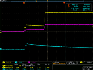
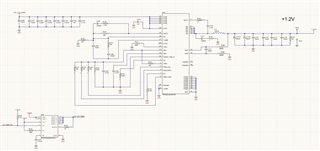
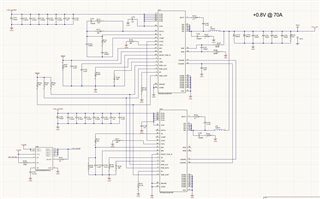
I have a design in which I have two separate supplies using the TPS546C20A to produce +1.2V and +0.8V.  I haven't turned on the +0.8V supply until I understand the behavior of the +1.2V supply.  I captured a waveform on my oscilloscope that shows the +1.2V supply coming up to +1.2V....then ~8ms later, it jumps to +3.3V.  In my design, I have the VSEL pulled up with a 10K ohm resistor to BP3.  Then, I have two 10K ohm resistors connected from DIFF0 to FB...and FB/DIFF0 to GND to produce +1.2V.  I measure the 0.6V at the FB pin as I expected...then did see a +1.2V at one of the 10k's.  What would cause the output voltage to be overridden from +1.2V to +3.3V?

Thanks,

Jeffrey McCasland

  • Hi Jeffrey,

    Can you please measure the FB voltage? Does it change from 0.6V to 1.65V, or does it stay constant at 0.6V?

  • Hello,

    What is strange is that at the moment I do see 1.2V at startup...the FB voltage is ~0.25V.  When the supply jumps to 3.3V, I see 0.6V that stays constant.

    Jeffrey

  • I do have an oscilloscope screen capture image at startup if there is a way to share a photo with you.

  • Hi Jeffrey,

    Yes, please share the oscilloscope screen capture. You should be able to insert a picture here (go to "Insert" and "Image/video/file").

    Also, please share the schematic. Thank you.

  • Here you go.  I've also attached my +0.8V design which behaves quite differently.  It will begin to charge to +0.8V...then quickly drive back down to ground. 

    FYI...I also have quite a bit of capacitance on my FPGA power I/O page..~1500uF per supply...

    Thanks for your assistance!

    Jeffrey McCasland

    !

  • In my 1.2V design, I'm tying VSEL to the +3.3V regulated output, BP3.  If the regulator doesn't lock, could this cause the output to 'rail' to +3.3V? 

    Also, my 'turn-on' of the regulators is done by turning ON the +12V input.  Given that I'm depending on the internal pull of CNTRL to enable the regulator, does this cause the startup issue?  i.e. do I need a valid +12VIN BEFORE deasserting CNTRL?

  • Hi Jeffrey,

    If VSEL is pulled up to BP3, the VOUT_COMMAND will be whatever value is stored in EEPROM. So I don't think there is any issue there, but please try valid 12VIN before asserting CNTRL and see if that fixes the problem. 

    However, I see a few concerns in your schematic, which may be causing the issue. Please make the following changes:

    1. The resistors in series with RSP/RSN traces should be 10 to 100 ohm, but the schematics have 49.9K. So please change it to 49.9.
    2. Soft start has a discrete setting, and 8.66K is not a valid resistor value. Instead, please use the appropriate resistor values from Table 3 of the datasheet.
    3. If RESETn/PGD pin is not used, leave it floating.

    We also have an Excel design calculator with a schematic and layout checklist: https://www.ti.com/lit/zip/slurb05

    Please use it to check your design.

    Thank you.

  • Hello Tomoya,

    Such ridiculous oversight on my part.   I implemented the items you mentioned in your response.  I also modified my design to NOT rely on the default value of VOUT_COMMAND (i.e. added resistor to VSEL to for 0.8V...then added feedback resistors to create 1.2V output).  Additionally, I added a mod to allow the +12VIN to go directly to regulators with CNTRL being driving directly from my power sequencer IC.  The result:  the +1.2V output comes up perfectly!  

    However, I still have some issue with my 0.8V design.  In this design, I have two TPS546C20As connected in parallel to create a 0.8V/70A supply.  I see the 450kHz SYNC signal between the two components. The ISHARE, VSHARE, and SYNC pins are connected per the TI data sheet for current sharing.  However, the output appears to have a 'hiccup'.  The voltage comes up to 0.8V...then, capacitively falls to 0 at a very slow rate.  I'm wondering...do the master/slave components NEED to have differing start-up times (via the SS pin)?  In one TI reference design, I saw the master/slave SS resistor the same.  In another reference design, I saw the master SS resistor set so that it comes up BEFORE the slave comes up...i.e. the master SS resistor set such that it comes up in 5 ms...the slave SS resistor set such that it comes up in 7 ms. 

    Does the master need to be up and stable BEFORE the slave?  

    Thank you so very much for you assistance!

    Jeffrey McCasland

  • Hi Jeffrey,

    The 2-phase application diagram in the datasheet shows SS and VSEL pins open for the loop slave device, so I would suggest leaving it open. 

    Did you make the same changes from the 1.2V design to your 0.8V design? If so, could you send me the updated 0.8V 2-phase schematics?

    If you're using PMBus, please check the STATUS registers to know which fault/protection the device triggered. 

    Also, could you share the oscilloscope capture showing SW, VOUT, VSHARE, and CNTL? This will help us with the debug process.

    Thank you.