This thread has been locked.

If you have a related question, please click the "Ask a related question" button in the top right corner. The newly created question will be automatically linked to this question.

LM61460-Q1: Regarding VIN UVLO Function

Part Number: LM61460-Q1
Other Parts Discussed in Thread: LM61460

Hi Team,

I am reading D/S and I am confused by VIN UVLO functionalities and VCC UVLO threshold. Could you please share your comments below respectively? Thank you.

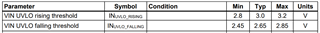
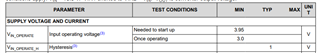
1.D/S says VIN has 3.95V for start-up and it needs at least 3.0V once operating. Is there any UVLO protection relating to VIN pin individually? This means, if I have VBIAS=5V, EN=HIGH however VIN down below 3.0V. Will device stop switching and enter shut-down? I am kinda wondering maybe VIN pin does not have UVLO. Its UVLO relies to VCC UVLO.

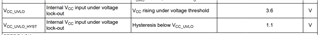
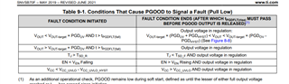
2.VCC UVLO. Is 3.6V and 1.1V relating to INPUT VOLTAGE of VCC, or VCC's output voltage? If so, what does table 9-1 mean? It says VCC<VCC_UVLO-VCC_UVLO_HYST. So it means VCC's output voltage is below its input voltage UVLO?

-A

  • Hi,

    1. In this case the device will turn on once input voltage is about 3.95V but during the descend, the input can be as low as 3V before the part stops switching. Note that " the simplest way to enable operation is to connect EN/SYNC pin to VIN allowing self-start-up when VIN drives the internal VCC above its UVLO level." Generally it is not recommended to have EN high while VIN is low voltage. Most applications will have EN/SYNC connected to VIN through a UVLO divider or directly tie the pin to VIN for self-start-up. Looking at the functional block diagram, you will see VCC_UVLO part of the LDO and softstart circuit. 

    2. The last entry in Table 9-1 states that if the Vcc voltage is below 3.6 - 1.1V = 2.5V, then the internal circuitry will not be internally turned on and the device would not switch. Only after the Vcc voltage clears the Vcc rising threshold of 3.6V and VOUT is regulating will the PGOOD flag assert high.

    Regards,

    Jimmy 

  • Hi Jimmy,

    Thanks for your comments. I have further questions about #1 and #2.

    1.

    1)So VIN does have input UVLO. However, 3.95V is the minimum input rising UVLO. The typ. and max value would be larger than it, which means VIN needs to be higher than 3.95V to turn on device. Is this correct?

    2)Also the falling threashold typ. and max value is higher than 3.0V, which means device may be disabled before VIN drops below 3.0V. Is this correct?

    This is important because in our application we have safety requirements, if VIN shorts to GND while VBIAS=VOUT, EN=HIGH, when VIN UVLO does not function correctly, this will cause unpredicable issue.

    2. It says VCC's typical voltage is 3.3V. How comes it could reach to rising threshold of 3.6V?

    Also it says internal VCC INPUT voltage. Does it means input of the LDO?

    -A

  • Hi A,

    Let me ask the system engineer to get further insight on this for the electrical characteristic table.  

    What is the customer's schematic and are they using a EN UVLO divider? If so then the turn on and turn off voltage can be calculated with the equation 13 shown in Section 10.2.2.11

    If they are tying EN directly to VIN, then the part should start up once EN clears the Ven rising threshold. Details of enable are shown in Section 8.3.2.

    Regards,

    Jimmy

  • Hi Jimmy,

    I am looking at LM61460-Q1 and MPQ4436 simultaneously, for the 13.5V to 5V/6A rail. I want to check how low the device can really go without protection. 

    Now the MPQ4436 seems to have lower VIN UVLO falling threshold than LM61460-Q1, which makes me wonder if it can be better with scenarios like cold cranking.

    Please help check the VIN and VCC specification per my last post. Thank you for your help.

    -A

  • Hi Albert,

    I have some feedback from the system engineer:

    1. The part’s UVLO actually senses VCC rather than VIN so the part will not be disabled if VCC remains above about 2.6 V.  During startup, the part only uses VIN and not BIAS so behavior will be different if the part is already running or if it is shut down then enabled with grounded VIN.

    2. VCC must exceed 3.6 V (typ) for the chip to start operating. Once this threshold is exceeded, VCC is regulated to 3.3 V in CCM and 3.15 V PFM. 

    The VCC is actually the output of the LDO. Please refer to Section 9.3.6 for details. " The VCC pin is the output of the internal LDO used to supply the control circuits". Also note that "If bias voltage is less than 3.1V, VIN1 and VIN2 directly powers the internal LDO". This means that both BIAS and VIN are the input (depending on which one is used) and VCC is the output of the LDO.

    Regards,

    Jimmy

  • Hi Jimmy,

    Thank you for your help. It is more clear now. Could you please check if my understanding below is precise or not?

    1. When start-up, before a signal (maybe PG?)=1, LM61460Q only uses VIN to supply VCC. When VCC's voltage is above 3.6V and EN=1, device attempts to start up;

    2.After PG=1, VCC is regulated to 3.3V in CCM and 3.15V in PFM. VCC's supply is switches to VBIAS or VIN which is lower;

    3.When VIN is droppping, VOUT also drops, when PG=0, VCC's supply switches back to VIN;

    4.When VCC's voltage drops below 2.5V or EN is below falling threshold, device is disabled.

    -A

  • Hi Jimmy,

    Another questions is, if I mannually supply VBIAS=5V and EN=1, can our LM61460 supports VIN=2V to 1V scenario? This is very impressive!

    -A

  • Hi Albert,

    There is a diode from VCC to VIN, so if VIN < VCC – VBE then the VCC capacitor will be discharged through the said diode. I don't think VIN = 2V would be valid scenario.

    As such it is suggested to stay within the datasheet specification of 3V input once the device has properly started up and is operating.

    Regards,
    Jimmy