This thread has been locked.

If you have a related question, please click the "Ask a related question" button in the top right corner. The newly created question will be automatically linked to this question.

TPS2115A: Automatic input switch for similar voltage input levels.

Part Number: TPS2115A
Other Parts Discussed in Thread: LM66100, , TPS2113A, TPS2115, TPS2113, TPS2116

Hi, 

Our current application design requires two similar sets of 4.2V batteries as primary and secondary power sources.
Previously, we were first considering the LM66100  but, as reported, it does not perform well when we have similar levels for the input voltages considering a seamless transition:
(https://e2e.ti.com/support/power-management-group/power-management/f/power-management-forum/1066260/lm66100-auto-switching-power-mux-with-similar-voltage-input-levels)

Then, w
e have been trying some ICs from the TPS21xx family as initially suggested.

Considering components availability, the TPS2115A  (D0 D1 and STAT pins) was selected for testing and the next results were obtained for the following configurations
Left side Vout (yellow) and STAT(blue) pins. Right side VIN1 and VIN2 ( initial voltage of 4.8V):

 Cin1 = Cin2 =  47uF + 10uF,  Rload = 100Ohm Cload = 10uF.

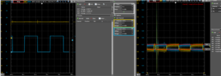
Cin1 = Cin2 =  47uF + 10uF,  Rload = 33Ohm Cload = 10uF.


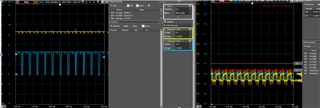
Cin1 = Cin2 =  47uF + 10uF,  Rload = 
20Ohm Cload = 10uF.


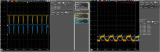
Result: Vout follows the highest VIN input when VIN1 >> VIN2 or VIN2 << VIN1 ( an output switchover voltage droop will still be visible).
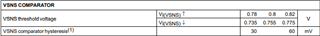
However, when both inputs are configured for a similar value, There’s a drop in the selected input, and the deselected input returns to its nominal value, (again the highest voltage). As shown, this causes an input oscillation (around 100mV) during the multiple selection. It might match the described comparator's hysteresis interval (
30- 57(typ) - 65 mV).

- Is there any suggestion on how to prevent this behavior and create a more stable output voltage?
- Is this device designed for an highest difference between inputs?
- Should the design approach be changed and only use the secondary power supply when the primary input reaches a pre-defined low voltage value ( i.e. using a resistor divider with the VSNS in version TPS2113A)?
- The D0 and D1 (TTL pins) on the TPS2115 version will not work as a comparator (similar to the VSNS), right?
- If using the pre defined voltage value, after the primary voltage source has switched to the secondary input source, will the device oscillate between both inputs when this secondary has the same voltage level as the primary source? 

Thank you for your attention.

  • Hello Fabio,

    I'll have a response for you by the end of the day.

    Regards,

    Kalin Burnside

  • Hello Fabio,

    TPS2115A does not have adjustable hysteresis and the only way to help prevent Vout from dropping more is by adding more output capacitance. If this isn't enough to solve the issue then you may want to use TPS2113 which is more efficient in auto-switching due to the VSNS pin or TPS2116 which you're able to modify hysteresis and it has a more modern switching method. TPS2115A is more often used for manual switching due to the D0 and D1 pins, though is definitely capable of working in auto-switching applications. Configuring the input & output capacitors becomes more of a balancing act. Let me know if you have anymore questions regarding this or any other pmux.

    Regards,

    Kalin Burnside

  • Hi Kalin,

    Thank you for your explanation.

    We will perform some tests using the TPS2113. But I would like to clarify the following topics:

    - Assuming that the resistor divider to define the switchover level (through Vsns pin) will be connected to VIN1,  what is the maximum resistance (MOhms) , or minimum current that should be flowing through the Vsns in order to have a stable switching point definition?

    - VSNS comparator hysteresis is described as 30mV to 60mV. Additionally,  the datasheet describes that the hysteresis is also 3.75 to 7.5% of the input voltage to prevent multiple transition of the inputs. I would like to better understand this behavior. Considering the  Vsns is configured through a resistor divider for a transition between Vin1 and Vin2 at 2.8V, what would be the worst case or limits for the transition if Vin1 = 5V, drops to ~2.8V and the Vin2 = 5V is selected?

    - Considering the Figure 14. Auto-Selecting for a Dual Power-Supply Application and the previous configuration for Vsns, IN1 will have priority and be selected again if its voltage goes > 2.8V, correct?


    Thank you for you attention,

    Best regards,
    Fabio.

  • Hi Kalin,

    Thank you for your explanation.

    We will perform some tests using the TPS2113. But I would like to clarify the following topics:

    - Assuming that the resistor divider to define the switchover level (through Vsns pin) will be connected to VIN1,  what is the maximum resistance (MOhms) , or minimum current that should be flowing through the Vsns in order to have a stable switching point definition?

    - VSNS comparator hysteresis is described as 30mV to 60mV. Additionally,  the datasheet describes that the hysteresis is also 3.75 to 7.5% of the input voltage to prevent multiple transition of the inputs. I would like to better understand this behavior. Considering the  Vsns is configured through a resistor divider for a transition between Vin1 and Vin2 at 2.8V, what would be the worst case or limits for the transition if Vin1 = 5V, drops to ~2.8V and the Vin2 = 5V is selected?

    - Considering the Figure 14. Auto-Selecting for a Dual Power-Supply Application and the previous configuration for Vsns, IN1 will have priority and be selected again (after IN2 has been selected) if its voltage goes > 2.8V, correct?


    Thank you for you attention,

    Best regards,
    Fabio.

  • Hello Fabio,

    There isn't a maximum or minimum resistance defined; however, we generally use 10k-100kΩ. The most important factor is the ratio between them and the ability to drive the 1uA current required (easily met) so I don't see any issues using MΩ.

    Whether it's on the 0.8V or the input voltage it'd be the same. You're looking at 3.01V-2.905V & 2.59V-2.695V. 

    Yes, you are correct.

    If you have anymore questions please feel free to reopen the post!

    Regards,

    Kalin Burnside

  • Hi Kalin,
    Thank you for the clarification.
    - What is the delay for the STAT pin state when a switchover occurs? Is it within the transition time or it occurs after the transition is settled?
    - Would it be possible to exchage priorities between IN1 and IN2 exchanging the R1 /R2 circuit connected to the VIN's after the transition ( using the STAT pin state)? In this way, after a first transition from IN1 to IN2 and replacement of the power source used in VIN1, the IC would give/keep the priority to VIN2 until it reaches the predefined minimum voltage level, and then switch to VIN1 again.

    Thank you!

  • Hi Fabio,

    1. The STAT pin is to change when the device makes the decision to change from one source to another. A good example of this is that, if the device is transitioning from a high voltage to a low voltage, the STAT pin will reflect the change but both channels could be off as the device waits for the output voltage to drop just below 3.3V to avoid backflow of current.

    2. The device is a black box, and will only work on the basis of the voltages on the SNS pin and the status of the EN pin. Any external circuitry can be used but the switchover condition is based on these voltage references. It may be possible to use the STAT pin to control external circuitry that changes the resistor divider network but I have not seen this done on TPS2113A.

    Thanks,

    Shreyas