This thread has been locked.

If you have a related question, please click the "Ask a related question" button in the top right corner. The newly created question will be automatically linked to this question.

LMR16030PEVM: Output voltage 24V drop

Part Number: LMR16030PEVM

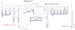
The following circuit is prototyped.
 Vin = 48V
 Vout = 24V

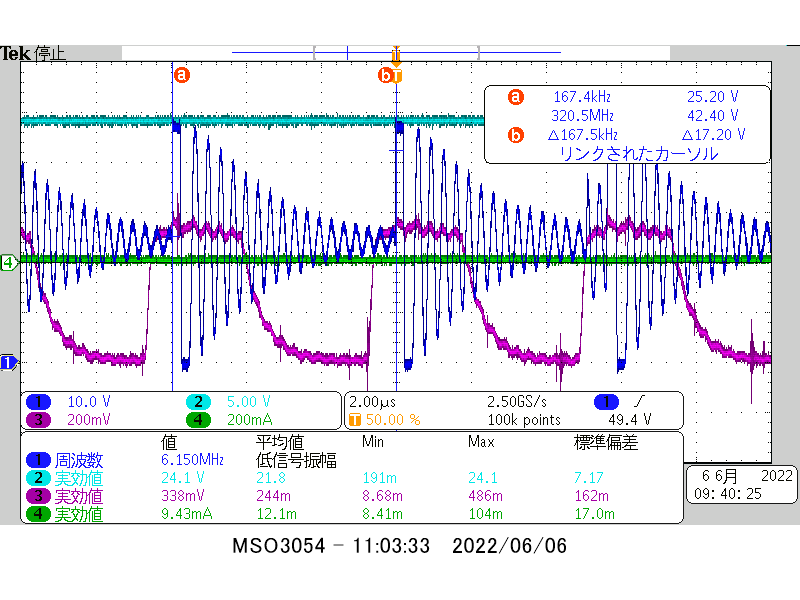
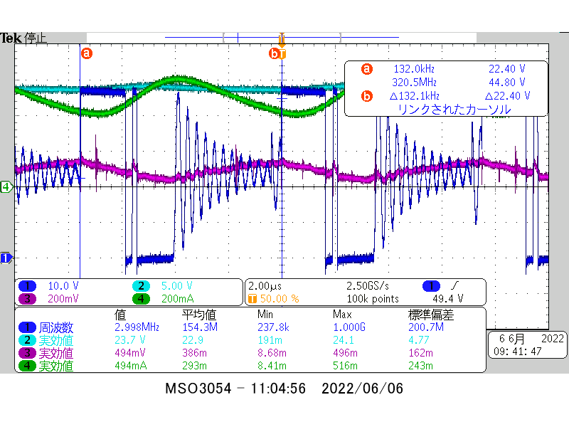
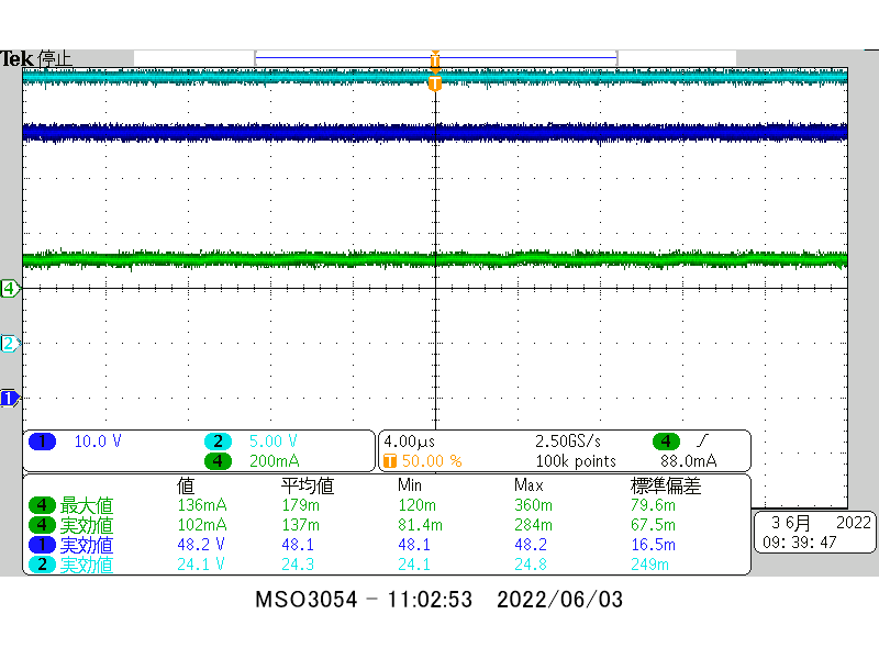
From the measurement results, the output voltage decreased according to the load.
 100mA = Vout: 24.1V
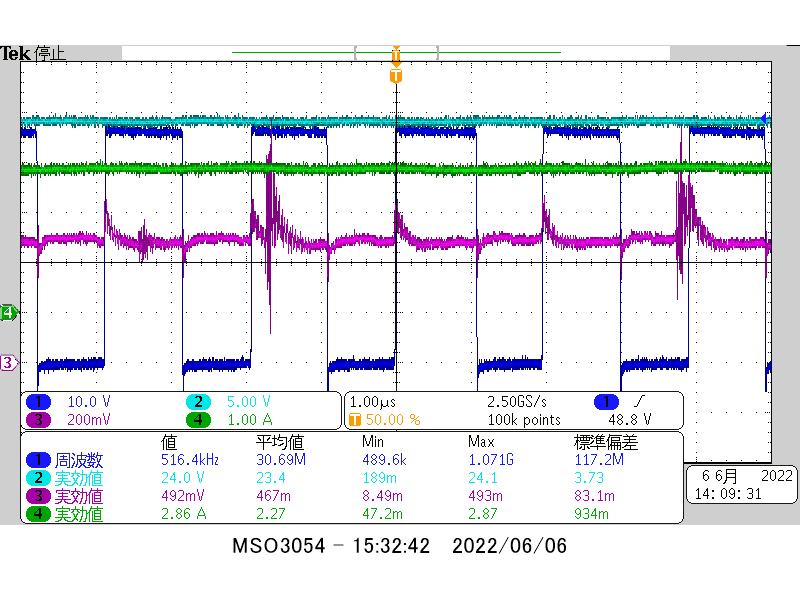
 500mA = Vout : 22.9V
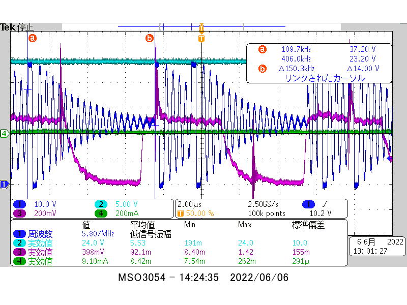
 1ch = Vin
 2ch = Vout
 3ch = Iout


If Vin=48V, Vout=24V, Iout=3A, and Temp=30°C are set in "WEBENCH", then Cff=560pF, it was better to change to 220pF.

After making this modification, I re-measured, but even under the condition of Iout=1A or so, Vout=22-23V.
Please advise me where I should make the correction.

Best regards .

  • Hello,

    Could you measure Vsw in these measurements?

    In the first plot, my guess is you are operating in DCM, so the device output is stable.

    With the higher load current, you transition into CCM, and due to an insufficient schematic you are unstable.

    I see the output capacitor has an ESR of 1.85ohm from the tan δ specification. This is quite high and could cause instability for this internally compensated regulator.

    My recommendation is, to un populate the CFF capacitor and locate a capacitor with an esr being << 1ohm (as small as possible).

    I see you can obtain Hybrid Aluminum electrolytic capacitors, 100uF, 50V, with ESR of 28mOhm. This would be much more ideal I presume.

    p/n:HZA107M050G24T-F

  • Thanks for the reply.

    I measured VSW.

     1ch = Vsw
     2ch = Vout
     3ch = Vrt_RT_SYNC
     4ch = Iout

    case1
    Iout ≈ 0A

    case2
    Iout ≈ 500mA

    The design value is the switching frequency ≈ 500 kHz.
    However, the actual measured switching frequency has changed depending on the size of the load.
    Please advise me how to correct it.

    Also, please let me check the contents of the circuit I received.
    Is it correct that the following two modifications are recommended?
       Cff(C54) : 560pF => NotMount
       Cout(C55) : UWT1V101MCL1GS => "ESR << 1ohm"

    Best regards.

  • Contact the result when cff is unimplemented.

     1ch = Vsw
     2ch = Vout
     3ch = Vrt_RT_SYNC
     4ch = Iout

    Case 3
     Iout≒2.9A

    Case 4
     Iout≒0A

    From this, if Cff is unmounted, Vout = 24V as configured.
    On that basis, let me ask an additional question

    a.
    Does the phenomenon "cff=implemented => phase margin margin decreases => switching frequency as set cannot be produced" occur?
    b.
    Is it appropriate to use the configuration "add a bias capacitor between +Vfb and GND with cff=not mounted"?
    c.
    When there is no load (Iout≈0A), I think it will be in DCM mode. At that time, is it correct that "Vrt_RT_SYNC" produces a pulse wave like in case 4, 3ch?
    d.
    I think there is noise in "Vrt_RT_SYNC". What can I do to reduce it?
    e.
    Is the "RT formula" in the datasheet correct?

    Best regards.

  • Hello,

    The switching frequency reduces in a light load mode. In CCM operation, the device should operate at a constant frequency.

    Yes, I recommend no mount CFF and using a low-ESR hybrid polymer electrolytic output cap, or, ceramic output cap.

  • A. Your ESR of the output cap introduces a zero into the loop. An additional zero is added with the CFF (which is also very large), causing you to crossover at an unattended frequency.

    B. A bias capacitor is optional, whether or not a CFF capacitor is utilized.

    C. Probing RT can infract disturb IC performance. It is a sensitive node. From a layout perspective, the best thing you can do is keep the trace from RT to its resistor small.

    E. Yes, I believe this is related to your earlier post?

  • I have a question about the A. that you replied to, which can cause crossover at unintended frequencies.
    In terms of the block diagram on page 9 of the datasheet, please tell me which part of the block diagram causes the unintended crossover.
    Also, I would like you to explain this phenomenon a little more. (You can give me the reference page if you want.)

    From your answer, I imagine the following, is this correct?
    The FB pin is connected to the error amplifier inside the IC with negative feedback.
    ESR capacitor = primary delay element, Cff = secondary delay element, and if the phase is shifted 180°, the error amplifier oscillates.
    This oscillation results in a crossover to an unintended frequency.

    Best regards.

  • A. the device's internal compensation intends the crossover to come at a reasonable (1/10 of fsw) frequency. 

    See this article right above section 2.5

    The ESR value of C75 is what is concerning.