This thread has been locked.

If you have a related question, please click the "Ask a related question" button in the top right corner. The newly created question will be automatically linked to this question.

TPS628512: TPS628512

Part Number: TPS628512

Hello,

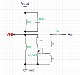
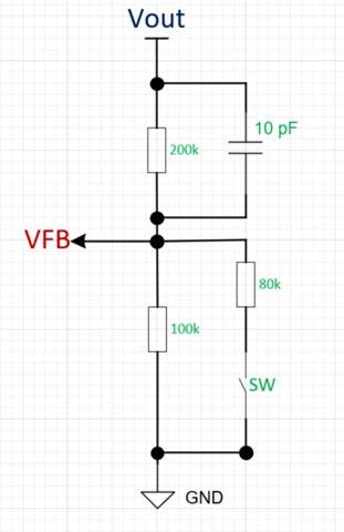
I want to output two different voltages(1.8V and 3.3V) from 1step-down converter, hence I added a header in the design as follows:

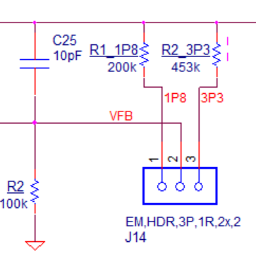
However, in the layout design it is mentioned that the trace to FB should be short. Is my design correct for this part or do I need to find another regulator?   

  • Hi Isha,

    It would be best to place the FB resistor dividers as close as possible to the IC to avoid any noise being coupled to the circuit. Hence, I'm proposing the circuit diagram below because the placement of the SW terminal (SW) will not affect the device operation. The Ra and Rb values depend on the Vin level.

    Do you think the circuit will fit in your application?

    * 80k resistor and 2N7002 needs to be placed close to the IC

    SW = Off: Vout = 1.8V

    SW = On: Vout = 3.3V

    Best regards,

    Excel

  • My application is an adapter board, which is a low current application and I am not expecting much noise. I currently don't have the layout, however I was wondering how much effect will this circuit have with respect to noise as compared to header. Also, will this header design work?

  • Hi Isha,

    Thanks for the quick response.

    Yes, all feedback resistors need to be placed as close as possible to the IC. The concern is the noise coupling  from other parts of the circuit. If you are confident that the feedback circuit will be noise-free, then you can use the header.

    By the way, you can also consider placing the switch on the low-side FB resistor so if the terminal is left floating, the Vout will be 1.8V only (see figure below).

    Best regards,

    Excel

  • Hi Excel,

    I think this circuit works for me. Installing a jumper instead of a 3 pin header can reduce the trace to FB. Thanks a lot!