Other Parts Discussed in Thread: LM5152-Q1, LM5176, CSD18563Q5A
E2E,
I have a good number of questions though my most pressing question has to due with the compensator components generated by the quickstart calculator and/or my interpretation of them:
Ranges:
IOUTmax = 6A
VOUT = 12V
VIN ranges from 7.5 to 12.6V
Questions:
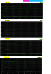
1. When using the quickstart calculator (see attached) to determine compensator components I get unacceptable inductor current ringing with a fbw range of 1, 5, 10 and 15 kHz when VIN = 12.6V. Note: I do not have a ringing problem at a VIN of 7.5 or 10.8V:
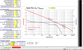
The part's datasheet suggests the fbw should be set to less than 1/3 of the RHP zero frequency (see equation 42).
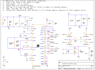
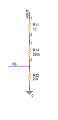
The current schematic (see attached "schematic.png") contains a snapshot for the comp components with an fbw of 10 kHz.
I also zipped the current state of the simulation in the attached zip file (assuming it is not to big for this forum).
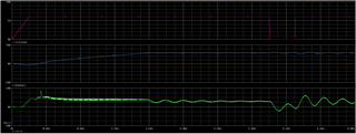
The results (see attached "ringing.pdf") pic contains the simulation results for the range of fbw listed above.
It is pretty clear in the worst simulations that the inductor current is ringing even before the load current step occurs.
Based on the quickstart loop gain, the phase margin should increase with decreasing fbw; however, ringing is low at 10 kHz then high again at 5 kHz. There appears to be a sweet-spot which the quickstart loop gain plot does not cover.
Not sure if I made a mistake setting up the simulation though my setup appears to match the quickstart setup/entries.
Any thoughts how to get past this problem?
All steady-state operating points have to pass simulation before I can move forward with this part. I had good results using the TI LM5152-Q1 quickstart calculator.
2. LM5176 transient PSpice model requires resistor (R1 = 2kohms) from VIN/Vsupply to VISNS pin.
Datasheet: "7.3.7 Operation Above 40-V Input
For an application where input voltage is higher than 40 V, a 2-kΩ resistor in series with the VISNS pin is
required as shown in Figure 8-1."
My VIN/Vsupply ranges from 7.5 to 12.6 V so the 2kohm resistor should not be required.
Is this a bug with the Pspice model or is the part's datasheet written wrong?
3. PIN PGOOD appears to have an allowed ISINK(PGD) range: 2, 4.2, 6.5 mA (min, nom, max) (see part's datasheet, page 8)
The part's datasheet, figure 8-1, employs an RPGOOD of 10kohms connected to VCC which ranges from 6.95 to 7.88 V (min, max)
This is how I interpret the current through RPGOOD:
IPGOOD = VCC/RPGOOD = 0.695mA, 0.788mA which are both less than ISINK(PGD) min.
Perhaps I am misinterpreting ISINK on PGOOD.
How exactly should I interpret/determine if I have chosen an RPGOOD value which violates ISINK(PGD)?
I'd prefer to connect RPGOOD to 3.3VDC instead of VCC.
4. The part's datasheet and its corresponding EVM design appear to employ a tss (soft start time) of approximately 16ms.
A 16 ms start-up time seems pretty long (I am using a 0.1ms starup time for the LM5152-Q1 boost controller).
Is there a minimum recommended start-up time for this part?
What is the rational behind a 16 ms start-up time? Perhaps some industry standard???
5. The part's datasheet and its corresponding EVM design appear to employ filter components (RC) between the RSENSE resisor and
the CS/CSG pins. The LM5152-Q1 datasheet has similar filter parts though does not appear to offer equations to properly size these
filter components. It appears as though this part's datasheet, quickstart calculator nor EVM does not offer equations to properly
size these components either.
I do not believe that the part's datasheet offers enough info to properly size these parts and I am guessing there effect on
the final value of RSENSE. Generally current sense filter increase the sense resistance i.e. RCS = (R1/R2)*RSENSE.
Would you please recommend a TI application note which properly sizes these current sense filter parts?
6. FET gate resistance:
The part's quick start guide lists 1.5 ohms for all four fet's gate drive resistances.
How exactly were these values determined? Perhaps TI has a good application note?
7. FETs:
The part's quick start guide lists the TI CSD18563Q5A (buck leg) and CSD163215Q (boost leg).
The TI part LM5152-Q1 employs the following to help pick FETs:
Equation 1: IG = 2*QG@5V*fsw and,
IG < IVCC_CL, where IVCC_CL = 100mA, and VCC ranges from 4.75 to 5.25
Know the range of VCC and the maximum QG@5V one can limit fet selection then make a final decision based on switching losses.
Does TI offer something similar for this part?
This part's VCC ranges from 6.95 to 7.88 V which limits VGS.
Perhaps I could use IHDRV1,2 (drive or sink) times a fets corresponding tr and tf, derive a minimum Q (Q = A*second) then
set that Q value as a minimum QG as a test for fets.
Does this sound correct?
Perhaps TI can recommend something similar to what part LM5152-Q1 does as listed above?
Thank you,
Craig