This thread has been locked.

If you have a related question, please click the "Ask a related question" button in the top right corner. The newly created question will be automatically linked to this question.

UCC256303: How to set Burst Mode Programming?

Part Number: UCC256303
Other Parts Discussed in Thread: UCC256403, TL431, PFCLLCSREVM034, UCC25630-1EVM-291

Hello,


I’m designing power supply system using UCC256303.

I want to decide the LL/SS-Pin's resistance (RLLupper and RLLlower).

UCC256303's data sheet is written (54page),

"Remove the RLLUpper. In this way, the VLL voltage is at its minimal value 0.7 V, which is determined by the internal circuit design. Then adjust the load current to the desired burst mode threshold load level, and make sure the power stage does not burst in this condition.".


I remove the RLLupper, but I cna not find the RLLlower' value.

How to decide the RLLlower resisrance?


Regards.

  • Hello, 

    Should I select this resistance value (RSSDown(222-580ohm))? 

  • Hi Tomohiro,

    I would recommend using design calculator finding LL/SS resistors : https://www.ti.com/lit/zip/sluc634

    Regards

    Manikanta P

  • Hello Manikanta,


    I used the design calculate sheet, but I can only write the V10k voltage value in the Maximum and the Minimum Input Voltage.


    I understand to use this steps for design the LL/SS value in UCC256303’s data sheet.


    Inserting a 10-kΩ resistor between the feedback optocoupler emitter and ground.( Assume the voltage measured on the 10-kΩ resistor is V10k.)

    Remove the RLLUpper. (In this way, the VLL voltage is at its minimal value 0.7 V, which is determined by the internal circuit design.)

    Then adjust the load current to the desired burst mode threshold load level, and make sure the power stage does not burst in this condition. (For example, 10% load is the desired burst mode threshold level. With 10 A as the full-load condition, set the load current to 1 A. )

    After the load current is set, change the input voltage to two different voltages and record two different readings (V10k, VBLK). (VBLK can be measured directly from BLK pin. )

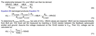
    ⑤ Then based on Equation 70 and Equation 71, RLLUpper and RLLLower can be solved.


    Is it wrong this steps?

    I want to find the RLLlower value in the step of .

    Regards.

  • Hi Tomohiro,

    First of all, we strongly recommend using our latest generation LLC controller UCC25640x which has much improved features compared to UCC25630x.

    RSSdown is internal to the chip. It has nothing to do with the burst mode threshold setting resistors.

    For setting burst mode resistors, you need to follow the steps as you described.

    Inserting a 10-kΩ resistor between the feedback optocoupler emitter and ground.( Assume the voltage measured on the 10-kΩ resistor is V10k.)

    Remove the RLLUpper. (In this way, the VLL voltage is at its minimal value 0.7 V, which is determined by the internal circuit design.)

    Then adjust the load current to the desired burst mode threshold load level, and make sure the power stage does not burst in this condition. (For example, 10% load is the desired burst mode threshold level. With 10 A as the full-load condition, set the load current to 1 A. )

    After the load current is set, change the input voltage to two different voltages and record two different readings (V10k, VBLK). (VBLK can be measured directly from BLK pin. )

    ⑤ Then based on Equation 70 and Equation 71, RLLUpper and RLLLower can be solved.

    You need to note down the two different readings of BLK pin voltage and voltage across 10k ohm for the same load (Example: 1A).

    So from equation 70, You have two equations and 2 unknowns. So, you need to solve those equations for for getting RLLupper and RLLLower values.

    Regards

    Manikanta P

  • Hello Manikanta,


    Thank you for teaching me about the RSSdown.

    Unfortunately, it is very difficult to obtain UCC256403 due to shortage of components on distributor.


    I execute the step and stop in step ③.

    Removed the RLLUpper and adjust the load current to desired burst mode threshold load level(48V/500mA(5%)).

    But, the circuit always work in burst mode.


    I changed VCR capacitance and FB optocoupler’s series resistance in reference to the following E2E design support, but I could not get good results.

    e2e.ti.com/.../ucc256303-skipping-pulses


    I set FB specifications as follows.

    FB optocoupler use TLP291(GB). (CTR=100~400%)

    U1= TL431BI, Vo=48V(target)

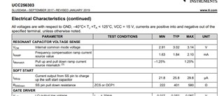
    R_f=15kohm, R_FL=560ohm, RUP=71.2kohm(47k+22k+2.2k), RLOW=3.9kohm, Rv=12kohm, Cv=47nF


    Other values were calculated by the following design calculate sheet.

     20220809_UCC256303_fo=200k.xlsx

     Could you help us why the controller is unable to get out of burst mode?

    Is there something else we are overlooking?


    Regards

  • Hello Manikanta,


    I examined the circuit more.


    I changed Rf to 47kohm from 15kohm.


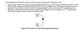
      And I added a bypass circuit between RVCC and FB pin in reference to the “UCC25630x Practical Design Guidelines”.


    4300.UCC25630x Practical Design Guidelines.pdf

    I selected the following values.

    Resistor : R=4.7kohm,

    Zenner diode : Vz=6.2V (KDZV6.2B)


    As a result, I was able to delete the burst mode, but the output voltage has become 60V.

    I design the output voltage become 48V.


    Would you help us how the I can clear the target voltage and delete the burst mode at the same time?


    I think I need to redesign the FB circuit.


    Regards

  • Hi Tomohiro,

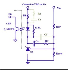
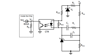
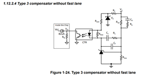
    The Fast lane of the feedback circuit connected to Vo or Zener diode (VDD)?

    Regards

    Manikanta P

  • Hello Manikanta,

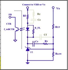
    Does "The Fast lane of feedback circuit" mean the point of "Connected to VDD or Vo" in the diagram above?

    If it is correct, we connected the Fast lane of the feedback circuit and Vo.

    Regards

  • Hi Tomohiro,

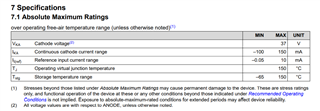
    You shouldn't connect 48V output to the TL431 without a zener diode since the abs max cathode voltage for this device is 37V.

    So make sure you connect a zener diode like below.

    Regards

    Manikanta P

  • Hello Manikanta,

    Thank you for finding my design's mistake.

    I'll give it a try right away.

    But, I have questions and requests.

    1. You told me about the TL431 and the zener diode,but I can't understand the relationship between TL431 and output voltage anomalies.

    Why would you think this would solve it? I want you to teach me that.

    2. Were there any other problems with the calculation sheet I sent before?

    The following are additional results.

    When the output voltage was 60 V, it was confirmed with an oscilloscope that the cathode voltage was 32.5 V. After that, the cathode voltage became constant at 2.5 V.

    Regards

  • Hi Tomohiro,

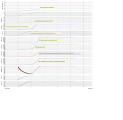
    Following waveforms should give you better idea why you should use a ZENER diode in a fast lane.

    These waveforms are taken from the simulation file (output voltage regulated at 12V) located at https://www.ti.com/lit/zip/slum684.

    Here You can observe that VK1 voltage across (cathode) follows the output voltage during startup until reference pin voltage reaches Vref (2.5V) which corresponds to ~48V in your case. So This indeed will exceed the Recommended cathode voltage of the shunt regulator and its going to be destroyed.

    So, You need to connect a ZENER diode as shown in my previous post. This would limit the maximum voltage across TL431 during startup.

    I think above explanation answers your both of your questions.

    Regards

    Manikanta P

  • Hello Manikanta,

    Maybe I have been able to solve the questions.

    Thank you for your help about this problem.


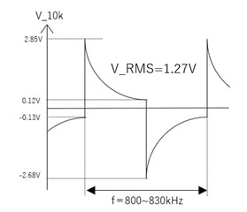
    I checked the 10-kΩ resistor voltage between the feedback optocoupler emitter and ground.


    As a result, the max voltage = 2.58V, the minimum voltage = -2.68V and the RMS voltage = 1.27V.

    (Input 285V  Output 48V/600mA)


    I will set the burst mode threshold in 5% load(48V/600mA).

    Which value should I use to calculate the LL/SS-pin's resistance?

    Regards

  • Hi Tomohiro,

    Could you share your schematic with me. I would expect V_10k to be always positive since FB pin always supplies the current. 

    Regards

    Manikanta P

  • Hello Manikanta,

    I send the schematic and the calculation sheet.

    Could you please check these?

    20220819_UCC256303_Design Calculator .xlsx

    8836.20220819_LLC-schematic.pdf

    Regards

  • Hi Tomohiro,

    I have gone through your schematic.

    I would like to make one more suggestion in addition with adding Zener diode on secondary side.

    You can further tune the VCR capacitors such that VCR pk to pk can be 5V instead of 4V for the rated load. That should increase VCR pk to pk voltage when the converter is operating in lower power range.

    Regards

    Manikanta P

  • Hello Manikanta,


    I changed the VCR capacitor that the VCR pk-pk can be 5V.(C32:2460pF→1970pF)

    But, it was not improve.

    I think I will decrease the output power and increase the VCR capacitor more.


    I reviewed the FB circuit design with reference to the following data.

     slua836a.pdf


    Other day, the output voltage abnormality has occurred.

    I thought that it was caused by the fact that the R33 was too big or the R34 was too small.


    I think the following calculation:

    I_R34=Vf/R34=1.25/560=2.2mA (Vf: optocoupler’s forward voltage )


    Since 2mA is required to activate the optocoupler, we assume that the output voltage has reached 60V.

    Vout=R33*(I_R34+I_diode)33k*2.2m72.6V

    Vout72.6V


    Therefore, when R34 was changed to 10k ohm, the output voltage became 48V, but burst mode was regenerated.

    I_R33 =(48-Vf-Vref)/R33=(48-1.25-2.5)/33k=1.34mA (Vref= U5’s forward voltage)

    I_R34=(Vf/R33)=1.25/10k=0.125mA

    I_R33-I_R34=1.2mA

    I_diode =1.2mA


    Is this way of thinking correct?


    Would you tell us how you designed the FB circuit?

    Also would you tell us the point where I should be careful about?


    Regards

  • Hi Tomohiro,

    I will respond to you by tomorrow.

    Regards

    Manikanta P

  • Hi Tomohiro,

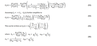
    Here is method i follow for feedback design:

    Place the wL close to 502rad/sec.

    wZ and Wp1 are determined based on the phase that you would like to add to the loop.

    Wp2 is high frequency pole to remove the noise.

    This is how I determine the feedback components.

    Regards

    Manikanta P

  • Hello Manikanta,

    What is the collector current of the optocoupler designed to be?

    The UCC25630x and UCC25640x's date sheets said "IFB>Iopt".
    However, when I calculated with UCC25630-1EVM-291 and PFCLLCSREVM034, I felt that "IFB>Iopt" was not possible.

    Regards

  • Hi Tomohiro,

    The collector current for the opto-coupler needs to be IFB max which is 164uA in case of UCC25640x (82uA supplied by internal current source and remianing 82uA will be supplied by FB internal current source when FB is clamped). In case of 30x, you can consider same value of 164uA (82uA supplied by internal current source and remaining current is supplied by the external zener clamp circuit)

    Regards

    Manikanta P

  • Hello Manikanta,


    I adjusted the FB circuit so that the FB voltage is at least 4V, but I have not been able to release burst mode yet.


    Therefore, we obtained SIMPLIS and analyzed the circuit by simulation.

    The SIMPLIS model of UCC256303 was downloaded from the TI website, but the following error was detected.


    *** ERROR *** (UCC256303_SIMPLIS_TRANS.net;138): Decryption failed: Unable to decrypt the data.

    *** ERROR *** (UCC25640x Simulation Test Bench.net;135): Decryption failed: Unable to decrypt the data.

    slum601.zip

    slum684.zip 

    Is there anything I need to do to run the simulation?

    Also, are these simulations not feasible in SIMPLIS_Elements (Demo)?


    Regards

  • Hi tomohiro,

    You can not run these models on Simplis elements. You need to have full version of simplis to run these models. 

    Regards

    Manikanta P