


Hi all,
We are working on a 1kW 400V/48V Dual-Active Bridge converter. To drive our MOSFETs in the primary and secondary side, we are using UCC21220 with the bootstrap configuration for each switching leg. The driver works well during forward power flow i.e. 400V to 48V bus in both open loop and closed loop. Now we are working on reverse power flow i.e. 48V to 400V bus. The system works well for open loop and closed loop till light load. However, during no load conditions, the low side output of the gate driver keeps failing. Mostly the pins OUTB and VSSB gets shorted. Our control loop is working fine and there isn't any oscillations in the phase and hence the output voltage. Generally driver outputs of MOSFETs Q4 and Q6 keep failing. Can you suggest some protection techniques or probe into why the driver is failing? Attaching some images of our schematic and waveforms of Gate-to-Source Voltage during the failure.
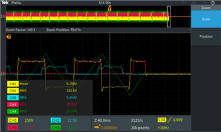
Figure 1: Waveforms during driver failure.
Red is the Gate-to-Source Voltage of Q4.
Yellow is the Secondary Transformer Voltage.
Blue is the Gate-to-Source Voltage of Q6.
Green is the Secondary Transformer Current.
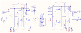
Figure 2: Schematic of Dual-Active Bridge converter topology with MOSFETs, Transformer and Leakage Inductor.
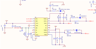
Figure 3: Schematic of Gate Driving circuit for MOSFET Q4.
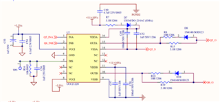
Figure 4: Schematic of Gate Driving circuit for MOSFET Q6.
