Other Parts Discussed in Thread: TPS54202
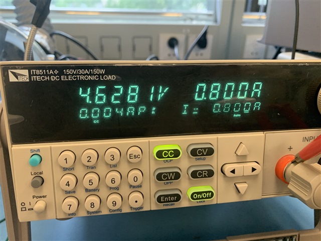
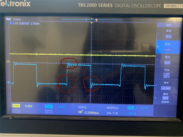
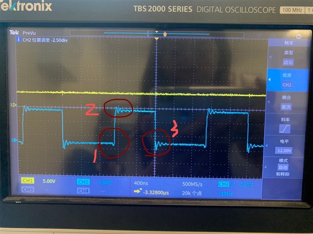
When I tested TPS54202EVM today, I found that when Vout=4.628V,Iout=0.8A, the waveform of Vsw is above. I don't understand where I circled out with a red line.
When I tested TPS54202EVM today, I found that when Vout=4.628V,Iout=0.8A, the waveform of Vsw is above. I don't understand where I circled out with a red line.