A related question is a question created from another question. When the related question is created, it will be automatically linked to the original question.
If you have a related question, please click the "Ask a related question" button in the top right corner. The newly created question will be automatically linked to this question.
UC3825 can be set up for VMC or CMC. When used in CMC, it sounds like you are already familiar with how to implement slope comp and if you prefer not to introduce slope comp then connect the full current sense signal into the RAMP and do not make any connection from CT to RAMP. Any time you add a portion of the CT "ramp" to RAMP you are influencing the sensed current signal ramp which is like combining VMC with CMC. If you want full VMC then you directly connect CT to RAMP and only use the current sense signal for OCP.
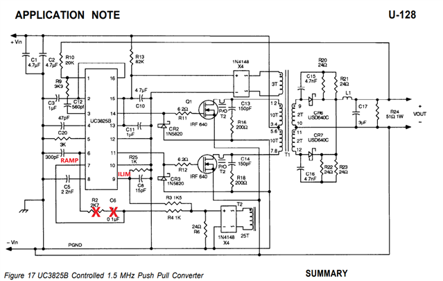
The schematic below is from app note SLUA125 and I marked it to show how would connect RAMP and ILIM without slope comp. It's not a buck converter but the same principle applies:
Good Day. Customer is not familiar with how to add the slope compensation to this IC. How does the scaling work, for example if he want to limit at 10A, would the current be scaled to 1V? Can you explain? Please advise. Thank you very much.
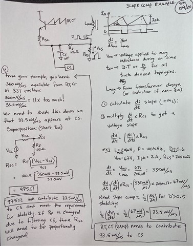
Slope compensation operation is a simple concept that follows the principal of superposition we learned from the college days. We consider two voltage sources where source1 is the VCS signal and source 2 is the RAMP. We calculate the contribution from each when the opposite is shorted - short source 1 to GND and calculate voltage 2 at VCS, short source 2 to GND and calculate voltage 1 at VCS, then add voltage 1 + voltage 2 to get the total VCS. The contribution from each voltage source is ratiometrically controlled by the selection of the RAMP resistor and the filter resistor (part of the RC current sense filter) both feeding onto the VCS signal. The two contributions are really summed at the current sense filter capacitor. Below is a worked out example I did for another customer. This was for a single-ended converter but the idea of slope comp is similar for a push-pull (note: the collector voltage on the BJT is not shown but this would be connected to VREF). What is shown below is a simplified summary of more detailed app notes TI has discussing the topic...SLUA110
Good Day. So the maximum duty cycle is at the lowest input voltage. If the customer have 80V in and 28V out, D is 0.35. Since it won't exceed 50%, are the calculations the same? When calculating di/dt, the graph you have starts at 0. The buck at steady state has a dc offset. Is just the ac part used for the calculation? Please advise. Thank you very much.
If Dmax=0.35 at VIN=28V then you don't need slope comp (in theory) but yes, the calculations for adding it are the same as what I showed. For calculating the inductor slope ignore the DC component. The example starting from zero just make is easier to explain/visualize. The inductor slope in CCM is constant by the volt-second balance, (Vin-Vout)*ton=Vout*toff. Are you using TI Power Stage Designer? This is a good tool for getting a quick view at the ideal power stage waveforms for any topology operating in any control mode. It's also helpful for control lop compensation modeling.
In the example given, it has 360 mV/uS available from RT/CT at the BJT emitter. How did you calculate this number?
The "B" is a revised part that buffers the oscillator to the CLK/LEB pin. Should this be used in the slope compensation instead of the CT pin? If so, are the calculations the same?
You have two slopes you are dealing with: (1) the natural slope on the CS which is the sensed inductor current slope (+m in my example) (2) the artificial slope of the RAMP from the PWM oscillator (360 mV/μs in my example). We only want to add a divided down portion of this 360 mV/μs to the CS - your case is probably not 360 mV/μs but is based on your oscillator frequency setting. The external BJT in my example is to buffer the RT, CT from the CS so we don't load down the RT, CT and cause a shift in oscillator frequency setting. If you are using a PWM that has an internal buffer then you won't need the external BJT I am showing.
Good Day. Please see the reply from the customer. Thank you very much.
I see many articles that say use of the CT pin is not recommended.
"In UC384X designs, it's common practice to buffer the timing capacitor saw tooth via a bipolar transistor wired in the common collector configuration. This approach presents several drawbacks. First, the Ct node (pin 4) is a rather high-impedance node because low currents circulate to charge up the capacitor. Therefore, it's not recommended to connect any other elements to this node.
In addition, the Ct voltage swing is around 1.6 V. By inserting a bipolar transistor in series with the capacitor voltage, you subtract a Vbe of 0.65 V @ Tj = 25°C from a 1.6-V swing. That is to say, at high or low junction temperatures, given the -2.2 mV/°C silicon slope, your final ramp amplitude can vary quite a bit and needs compensation somewhere."
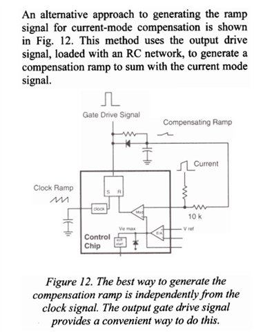
Many suggest using the gate drive output to generate the slope compensation. Have you had any experience with this?
The point about high impedance noise and low-currents implies the degree of care that should be taken in the PCB layout regardless if a BJT buffer is added to CT....careful grounding separation is important with peak current mode controlled converters. The use of CT for slope comp is sometimes not recommended because anything that loads the clock could introduce potential inaccuracies in the frequency setting. In the worst case, this could mean having to overdesign the power stage to compensate for a variance adding to what is already given in the data sheet over temp/process/tolerance. With that said, the buffered divided down circuit we've been discussing in this thread is still, by far the most popular because of it's long legacy attached to the popularity of peak current mode control stemming from over 30 years of use. Some of the sources citing not to use the CT pin are no doubt coming from IC innovation, integrating programmable slope comp that is independent of the RAMP signal or buffered internally - in such cases it makes perfect sense to highlight the deficiencies as a segway to an improvement.
The CT voltage swing of ~1.6V and the impact the BJT has should not have a first order effect on the RAMP peak-to-peak as far as PWM control is concerned. It could be said that additional signal routing near the RT, CT has an impact on signal grounding and yes, there will be a Vbe drop but this should only be seen by the summing node (CS filter cap) where the divided down RAMP is being applied. The small amount of slope comp needed for stability can easily absorb the Vbe drop with plenty to spare and should not be a concern. If you're adding that much slope compensation, you most likely have other problems such as shifting the converter too far into voltage mode control which you probably have not used the correct compensator if you were planning current mode control.
Regarding the use of the gate drive signal for generating slope comp, I am familiar and have successfully used it. Gate drive is another critical part of routing a PCB so now you must choose between disturbing the gate drive vs the RAMP. For low/mid frequency designs I've had good success with the RCD on the gate drive...even better if you can pick off the gate drive before feeding it into a gate driver totem pole or IC drive stage. You need a fairly large RC to get a linear ramp and a low Vf Schottky to discharge the cap. I tend to prioritize my gate drive circuits during PCB routing - I like to be able to control the gate drive turn on/off edges and make sure it's critically damped best as possible. I haven't seen the RCD gate drive slope comp as a hinderance to this but I'm also cautious that it could be.
Good Day. Additional inquiry from the customer. Thanks.
The enhanced version B has a buffer on the clock but it doesn't look like it's the same as the CT pin. I was thinking the CT node was buffered for the transistor, but it looks like that's not the case.
Is this good for a synchronous buck converter. I noticed the outputs switch alternately on the clock. If a diode was used it will come on after the transistor pulse goes down. Using this to control the transistor replacing the diode, it has to wait another clock cycle. Would doubling the clock frequency work? (200khz instead of 100 kHz to make it work like the diode)
Or is there a better part for a synchronous buck converter?
I hope that I've helped contribute to the original post about slope comp? Keeping the conversation close to the subject thread helps improve the search accuracy for the entire E2E community. Since this topic has shifted from the original post title, I'm going to close it and ask that if additional IC support is needed (choosing a sync buck controller), you can open a new thread with a thread title related to your inquiry? Thanks for connecting through E2E.