This thread has been locked.

If you have a related question, please click the "Ask a related question" button in the top right corner. The newly created question will be automatically linked to this question.

LM25148: schematic check

Part Number: LM25148

Hi

Could you help check the below LM25148 schematic and any need to adjust

lm25148.pdf

  • Hi Gareth,

    Please fill out and attach LM25148 quickstart calculator.

    https://www.ti.com/tool/LM5148-LM25148DESIGN-CALC

    Use the quickstart calculator to recalculate compensation components.

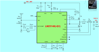
    12V output switching at 2.1MHz may see very large losses on the MOSFET. Check the high-side FET power dissipation with the quickstart calculator. If its more than 2 or 3 watts then I recommend lowering switching frequency.

    You cannot connect 12V to VCCX pin, you will damage the IC. Use a 5V rail if you have it.

    You may not need boot diode D5, LM25148 has internal boot diode.

    Is there a component on the current sense VOUT trace? The SP1 component tied to 12V_FB_N. I recommend removing that component completely.

    Hope this helps,

    -Orlando

  • Hi Orlando

    EXCEL has been filled out, please help to confirm

    1. How do I reduce the frequency to 300KHZ like EXCEL.

    2. VCCX cannot be connected to 12V, what should I do with VCCX? Can it be empty?

    3. D5 is not needed. Then CBOOT directly 0.1uF to SW?

    4.+V12A goes directly to PIN 21 VOUT. I am worried that LAYOUT will go directly to 1 POWER PLANE into PIN21. SP1 is a single wire NET component.

    5. PIN18 PFM/SYNC I am now VCCA connect 0R to PIN18. Please suggest me how to connect better.

    LM5148-LM25148 Quickstart Calculator_rev2 的複本.xlsm

  • Gareth,

    I'm not sure how you schematic got messed up, it might be your screen resolution is resizing the image.

    I opened the default excel and my image looks better.

    1. The change frequency to 3000kHz use a RT resistor of 73.2kΩ.

    2. VCCX should be tied to GND if not used. 

    3. Yes.

    4. Got it, yes please use traces directly from the current sense resistor Rs to the ISNS+ and VOUT pins.

    5. PFM/SYNC can connect to VCC or VDDA, or any voltage >2V to configure PFM (or <0.8V for FPWM mode). Just dont exceed the pin abs max of 6.5V.

    -Orlando

  • Hi Orlando

    The schematic modification is completed, please help me to confirm again.Thanks

    1781.LM25148.pdf

  • HI Gareth,

    Sorry for the delay as Orlando is OOO. Schematic looks decent. Please send the associated quickstart for review as well.

    Regards,

    Tim

  • A few notes:

    1. The VCC cap doesn't need to be 50V; 16V is fine. Smaller footprint cap is better as it allows tighter placement. Also, this might allow use of X7R instead of X5R dielectric.
    2. No need for the boot diode.
    3. Consider using a Pi-filter on the input for EMI.

    Regards,

    Tim

  • Hi Timothy

    The modification is as follows, please help to confirm whether it needs to be adjust

    Thanks

    5732.lm25148.pdf

  • Hi Gareth,

    I see VCCX is connected to V3.3A_LDO., this is a 3.3V supply.

    VCCX rising threshold is 4.3V (typ), a 3.3V supply will not work.

    I recommend tieing VCCX to a 5V supply or typing VCCX to GND if 5V is not available.

    Alternatively, you could use a something like a 6.8V Zener connected to 12V VOUT, so that the resulting VCCX voltage will be ~5.2V.

    Just be sure not to exceed the VCCX pin's ABSMAX.

    Everything else looks good to me!

    -Orlando