


Hi Expert
we have five question as below:
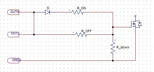
1. can we choose below way to design the OUTH and OUTL driver resisters?
2. what difference between VCECLP and DESAT?
3. if we needn't AI2~AI6, How to connect it? pie to GND?
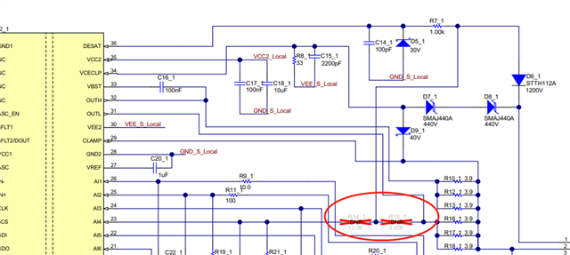
4. what function is below R14 and R15? what condition need to post it?
5: how to calculate decoupling capacitor in the VREG2 and VEE2? Is it must 4.7uF? customer want to to choose 2.2uf, is ok?
