This thread has been locked.

If you have a related question, please click the "Ask a related question" button in the top right corner. The newly created question will be automatically linked to this question.

LM5181: SW Pin and Vin ripple for different Modes of Operation

Part Number: LM5181
Other Parts Discussed in Thread: LM5180EVM-DUAL

Hi,

we have custom board with dual output flyback design based on LM5181 with following parameters: 

Vin nom= +12V

Vin range = 11V…13V

Vout1 = +12V /200mA

Vout2 = +56V / 5mA

Npr :Nsek1 = 2 :1
Nsek1:Nsek2 = 4.67:1

L = 110uH

Rpr = 0.268 ohm

Rsek1 = 0.066 ohm

Rsek2 = 2.8ohm

Dclamp = TVS SMAJ24A
Df= 30V 1A, Shottky  

Snubber elements on primary side were not populated during measurements.

Remark: the same IC on the custom board was previously used with 500mW 22V Zener diode as clamping diode. The diode was working on the limit and it could be the case where IC was working for a while as the diode was broken. Since the IC was not replaced with the new one, we don’t know whether we also have an issue with the damaged IC that cause following results.

We measured SW pin and input ripple for different load current conditions. Some waveforms correlate with waveforms that could be found in LM5180EMV-S05, LM5180EVM-DUAL or in SNVAA28 (+/-18V Dual output) for heavy load condition. 
However we have observed some strange behavior on SW pin for relatively small and medium loads between 25mA and 50mA where input ripple became quite higher as it was at heavy load. This lead to confusion as we tried to identify current Mode of Operation according to SW pin waveform which LM5181 currently work in. As it can be seen, the IC "jumps" between two operating modes even the load current was constant during the measurement time. 

We had started with 1mA load at output 1 and no load at output2 measuring SW pin waveform only. The load was applied in steps of 10mA. Afterwards we added Vin ripple waveform and additional measurements where the ouput2 was loaded with 1.8mA and 3mA loaded respectively. 

Could you advise us which of these 3 operating modes (FFM, DCM and BCM) the scope pictures Scope09... to Scope13... are related to? Is this normal behavior of sw pin where we have excessive ripple on the input voltage for some load values? 
Or do we have here perhaps an issue with minimum Off-Time?

Is the diagram Figure 8-2. from datasheet on the page 10 valid for any output configuration, regardless whether it is single output, dual output, positive output configuration, negative output configuration?
What the Total Rated Output Power is related to, max. power of used transformer or to the max. power that LM5181 can handle (Primary switching current)?
 
We have also observed that the SW pin has less stable switching frequency (up to 10% jitter) and for 100mA load the measured SW frequency is 151kHz. This is also confusing since according to the figure 8-2 from data sheet it should not be less than 225kHz.

Electronic load was used during the test and SW pin was measured with grounded lead on scope probe. Only scope picture Scope42… was measured with short ground spring.

There is also a some kind of swinging on the rising edge of the SW pin. For the light loads it is located in the middle of the rising edge and it moves upwards as load increases. It will disappear at 90mA load. 
Could you advise us where this swinging on SW pin could come from?  
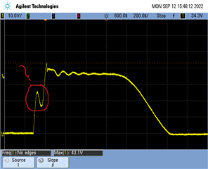
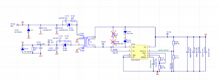
Schematic: 

Scope pictures: 
TVS_SMAJ24A_without_Snubber.zip

Regards
Josko


  • Hi Josko,

    Thank you for posting.  According to your description, D1103 for the primary side snubber was overstressed, because the flyback voltage would be 2x 12V=24V, greater than the 22V Zener voltage, not to mention the spike voltage during the switching transient.  I would like to suggest a ~32V Zener for D1103.

    Similarly, D1114 at the +12V output rail should be changed to ~13V Zener.  Otherwise it may be overstressed too during normal operation.

    Please also refer to our quickstart design calculator: https://www.ti.com/lit/zip/snvu075

    Regarding Figure 8-2 of the datasheet, it is a typical curve and it can change according to a specific design and operating conditions. The calculator will show actual frequency curve once you plug in your design component selections. 

    Jitter may also be layout related:  at reduced load, the circuit switch at a higher Vds of the internal MOSFET due to DCM mode, and the noise may cause jitter.

    Regarding the SW step, it may be related to the leakage resonating with the internal FET capacitance and a higher current would have stronger resonance magnitude. It is normal and not a big concern. 

    Hope this clarifies, and good luck in your design.

    Thanks,

    Youhao

  • Hi Youhao,

    thank you on quick response and information. 

    One question topic hasn't been commented. Have you seen attached scope pictures in zip file? 
    Could you comment on operating modes (FFM, DCM and BCM) and the scope pictures Scope09... to Scope13...? Is this normal behavior of sw pin where we have excessive ripple on the input voltage for some load values and suddenly changing operating mode for a constant load value (excessive ripple can be seen on pictures scope29..., scope34..., scope36...,scope37...)? 

    Do we have here perhaps an issue with minimum Off-Time?

    If we have FFC mode up to 20mA load current (picture Scope06_) and at 25mA the operation mode is transitioned from FFC to DCM (picture Scope07_...) , why do we have sudden jump back to FFC mode at 30mA(picture Scope09_...)? 


    Regards

    Josko

  • Hi Jasko,

    I just deleted my reply and here I repost:

    These seems being affected by the noise and an optimal PCB should help. However, this is not a very critical issue, because the IC still is still fulfill its function: regulating the output voltage.   

    As you may know, the circuit is regulated by sensing from the primary side and switching noises can lead to such intermittent mode change.  Please update the Zener clamp first, and redo the test, and see if some improvement can be obtained.

    Thanks,

    Youhao

  • Hi Youhao,

    just for information, measurements I sent in zip file have been already made with TVS diode SMAJ24A (TransilTm (farnell.com)) instead with 22V Zener diode MMSZ5251B-7-F.

    We will try either, fit our transformer on the LM5180EVM-DUAL and see whether there are some changes or made custom board with PSU unit only with improved layout.  


    Regards

    Josko


  • Hi Josko,

    Sorry I might have spelled your name wrongly several time.  Apology for that.

    We usually do not use a TVS for the flyback transformer snubber circuit, because its soft knee and less effective voltage clamp.  Please use a ~32V Zener diode as I mentioned earlier. 

    Also, please let me know your test results of mounting your transformer with our EVM. 

    Best Regards,

    Youhao

  • Hi Josko,

    Having not received any update for more than a week, may I assume the issue is resolved so I can close the thread here?  You are welcome to re-open this thread by adding a new post. 

    Good luck in your project.

    Best Regards,

    Youhao