This thread has been locked.

If you have a related question, please click the "Ask a related question" button in the top right corner. The newly created question will be automatically linked to this question.

TPS61022: Loop Instability Query

Part Number: TPS60122
Other Parts Discussed in Thread: TPS61022

Hi,

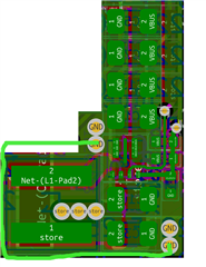
I have a TPS60122 boosting super-cap voltages up to 5v and anywhere from 0-3A. It's not using the reference design but follows the same principles. 

Spec:

Output: 4x 22uf/0805/X5R/10V
Input: 8x 22uF/0805/X5R/10V (2 very close, 2 close to the left of the inductor, 4 on the rear.
Divider: 732k/100k

I've had this circuit running before without any loop instability but the inductor was on the reverse, less than ideal and so it was moved. There is another shielded inductor from a 100KHz buck circuit on the rear of the board but there's two inner layers which are GND so (I think) this won't impact it.

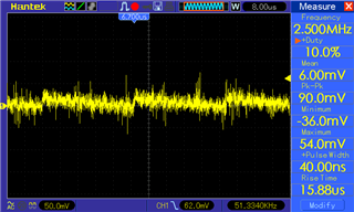
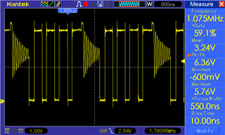
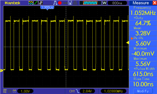
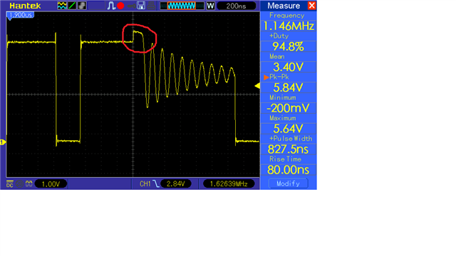
What I've found is with a slight draw of about 5mA from the output the voltage ramps from 5v to ~5.5v with huge noise, AC measured as ~100-400mV.

This is with the input voltage from 2.5v to 4v. I didn't test other values but I need to support 0.5-5V input, whence the decision not to use a feed forward capacitor.

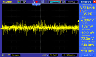
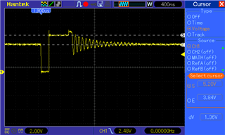
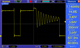
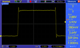
I've tried adjusting input & output capacitance up but to no avail. I then added a 330pF feed forward capacitor and the situation has fully resolved.

The question is whether this is going to limit the input voltage / output current that I can utilise, and the second question is whether using smaller feedback resistors (i.e 73.2k & 10k) will increase stability at the expense of a little extra draw, rather than use the feed forward capacitor which (I think) targets a particular voltage/current combo.

Regards,

Andrew


  • PS) the green line is showing where ground has a path on the green/rear layer but it's cut off in the image.

  • Hello, 

    Thanks for reaching out. Can you please clarify the specs of your system (Vout, load current and Vin range)? The TPS6012x is a 3V 200mA charge pump device, could you please double check the part number of the device you're using? We're looking forward hearing from you. 

    Kind regards,
    EM

  • That's why I wrote TPS61022. ;)

    Vout = 5V, load current = 0 - 5A, Vin = 0.7 - 5.15V

    Regards, Andrew

  • Hi Andrew,

    The feed forward cap will not limit input voltage or output current. And I think changing resistor divider have no impact on stability.

    And more, I have these quesitons:

    What the inductor value you use? 

    Do you have the instability waveforms? Like VIN VOUT SW node.

    Is there a pullup resistor of EN signal? If there is, what's the resistor value?

    Does the instability only appeared in IOUT=5mA?

    Thanks,

    Best Regards,

    Nathan

  • Hi Nathan,

    Inductor = Coilcraft XEL 4030 1uH
    Pull-up = No, it's driven hard by MCU
    Waveforms = I can get them, but I did look at AC analysis of VOUT with the instability where it rises to about 5.6V (hitting the TPS61022's internal limiter) and it was all over the place with no consistent pattern. The nominal draw of the MCU etc is less than 5mA but when some other items are turned on the draw is a bit higher and that's when the ~5.6V was noticed.

    With the 330pF feed forward I have since found with the input voltage at 4.6V and a significant amperage draw of 700mA it will only produce about 4.8V at the output. This seems to be quite a voltage drop. I then did an IR inspection and chip looks good. Apart from this voltage drop the stability across the input voltage range seems good.

  • Hi Andrew,

    Thanks for your information. 

    As for the VOUT drop problem after adding feed forward cap, you can put a 1kohm resistor in series with the feed forward cap. It will be helpful.

    And the instable problem, what do you mean that " AC analysis of VOUT with the instability" ? have you test the phase margin and gain margin? Or if you can provide unstable waveforms, it will be more helpful. Thanks.

    Regards,

    Nathan

  • I did surgery on the board inserting 1k as you suggested. The nominal voltage has now increased with minimal load now 5.15v (5v with 330pF, 5.6v with no FF cap).

    These are at minimal load, the MCU is powered, some some LED's. Expect it'll be 5mA max.

    AC analysis of output is reasonably clean, ignoring the spikes it's about 50mV or so, acceptable.


    AC analysis of input ignoring the spikes is similar, say 50mV. 

    So one thing first. If you look at the PCB above you can see that the input capacitors have a large trace to pin 1 ground. Although there are big vias it's probably not ideal. However, the datasheet uses exactly the same approach so I'm assuming that is not the problem.

    Now for SW. Again I'm only focusing on minimal load for now. As this is VBUS I can accept overshoot to 5.25v.


    You can see with the cursor that it's overshooting, at least in the light-load DCM mode. If it seems normal I can move on to higher current draw analysis.


  • I've done further investigation and it seems the 1k while adding overshoot at very light load has resolved the voltage sag under load. I pulled 1.2A at an input of 4.5v and received 5.04v, which is bang on. 

  • Hi Andrew,

    Could you please measure SW node waveforms in PFM with smaller voltage scale? I think 2V/div may be too big to figure out the 200mV error. Thanks.

    And more, I think the layout is fine.

    Nathan

  • This one is roughly 330mA output. It's switching between DCM/CCM.

    (This is with 330pF + 1k FF)


    Zooming in...


    At roughly 660mA it's CCM only...


    Zooming in...

  • Hi Andrew, 

    I think the waveforms you show are all fine, and the high level of SW node is also about 5V.

    Do you mean this overshooting? This is also normal behavior duo to the body diode voltage drop of high-side FET.

    Nathan

  • Thanks. So I'll stick with the 330pF + 1k res.  A little high voltage on very low current draw I can live with and the rest of the time it's stable.

    Thanks for your help,

    Andrew