This thread has been locked.
If you have a related question, please click the "Ask a related question" button in the top right corner. The newly created question will be automatically linked to this question.
Hi :
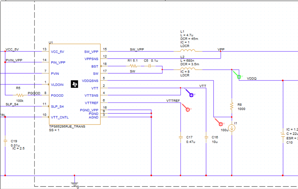
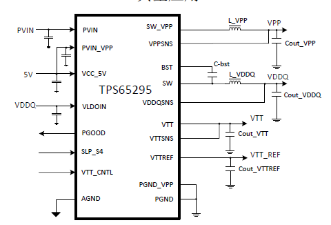
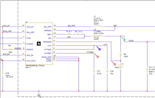
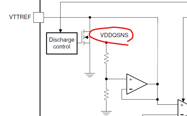
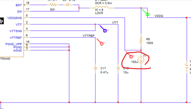
I am using TPS65295 IC for our DDR4 power solution.
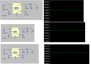
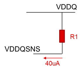
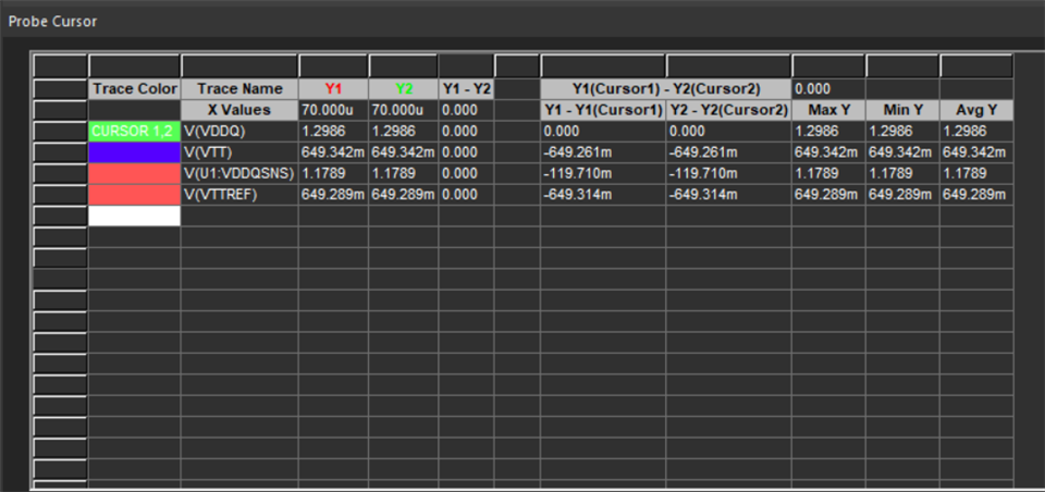
I would like to vary the VDDQ supply +/-3% (1.2V +/-3%) to characterize the DDR4 controller performance at corner voltage scenario.
Is there a way to change this beyond the typical limit of 1.2V ?
best regards
Shamanth
I would like to use above concept at VDDQ output path. VDDQSNS connected to VDDQ rail through a Resistor R , current source (DAC) connected to another end of Resistor . VDDQSENS voltage always maintained at 1.2V at closed loop scenario but output voltage VDDQ changed according to current and Resistance combination
Hi Shetty
The voltage of VDDQ can be increased through adding a resistor(R1) between VDDQ pin and VDDQSNS pin. VDDQSNS input current is 40uA according to datasheet, and the variation of VDDQSNS input current is -17%, +20%. VDDQ =1.2+R1*40uA.
Hello Zhang : Thanks for the information
I have Pspice simulation and attached the schematic and result
With this schematic configuration the VDDQ voltage increase to 1.298V( 98mV more than 1.2V)
The VTT and VTTRef = VDDQ/2 ---> ~649mV
But as per the datasheet VTT and VTTRef = VDDQSense/2
Please clarify ??
thanks and regards
Shamanth
Hi Shamanth,
As the datasheet 7.1 Overview shown, VTTREF tracks VDDQ/2, and VTT tracks the VTTREF.
In Electrical Characteristics table, VTTREF = VDDQSense/2, which applies for typical application below.
Hello : As per simulation shared above it is tracking VDDQ . But we got the EVK of this and tested in the lab. The VTT and VTTREF is following VDDQSENS
Please clarify - Is anything wrong with the spice model
Hi : I tried to understand VTTREF is tracking VDDQSENSE or VDDQ . Please clarify ? Measurement result in the lab and simulation result Pspice are providing different result .
Hello :
Please refer to my schematics
Pspice simulation :
VTTRef and VTT is tracking 1/2*VDDQ
Lab Measurement using TPS65295 EVK with same schematic changes as mentioned in the Pspice sim setup
VTTRef and VTT is tracking 1/2*VDDQSNS
Unable find out why there is a difference b/w Lab measurement and Pspice simulation result ? Also which result is correct
thanks,
Shamanth
Hi Shamanth
please see the 7.2 Functional Block Diagram of datasheet, exactly, the VTTREF is tracking VDDQSENSE. why do you add the I1? you can remove the I1 and try again.
Hello Zhang : The current source I1 added to vary the VDDQ voltage ( 1.2V +/- 10%) . I am able to find the expected result in both simulation and lab measurement. But lab measurement and simulation result are not matching for VTTREF and VTT
Hello Shamanth,
As your experiment turned out, we are also a little confused. We'll go to the lab to replicate this problem and discuss it with Design Team to see what went wrong.
Hi Shamanth,
Due to impact of the pandemic, we can't get back to you right now. If there is a conclusion, we will reply you as soon as possible.
Hi Shamanth
I have confirmed that the VTTREF is tracking VDDQSENSE and your lab results is correct. I not sure if the Pspice have some bugs. For example, we all know that the VDDQ=VDDQSNS by default on most typical applications, whether the incorrect internal setting that VTTREF = 1/2*VDDQ occurs, Recommend removing I1 first and checking again if the VTTREF is still equal to 1/2*VDDQ, because I'm not sure if the current of I1 will affect VDDQSNS.