This thread has been locked.

If you have a related question, please click the "Ask a related question" button in the top right corner. The newly created question will be automatically linked to this question.

TPS62903-Q1: TPS62903-Q1 datasheet

Part Number: TPS62903-Q1

Hi Team,

1. I was reading about datasheet of TPS62903-Q1. In 9.2.2.5.1 paragraph about output capacitor, here says 'Using higher value has a tighter DC output accuracy'. I'm confused that why and how the value of output capacitor influences DC accuracy? Is there any reason about loop gain as we all know high DC loop gain causes a high DC accuracy? 

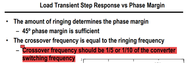
2. About compensation loop design in VM control mode Buck converter, some documents shows about we should set crossover frequency on 1/5~1/10 switching frequency which is a typical engineering experience. I wonder why crossover frequency(bandwidth) is related with switching frequency and what's the performance goal if we set crossover frequency as this?


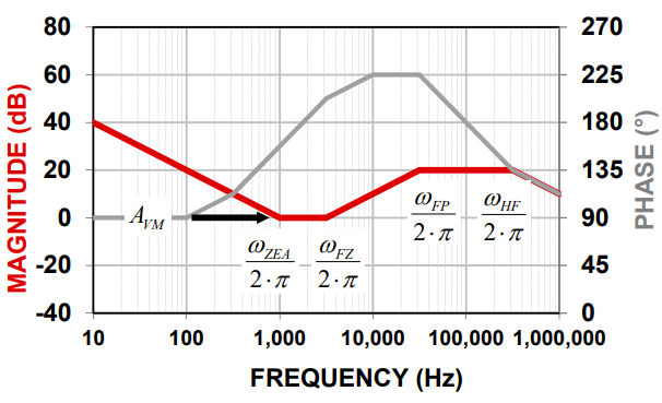
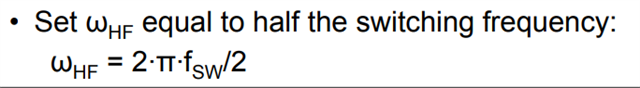
3. About the design of TypeⅢ compensator, the bode plot is as below. There is a wHF pole in the plot which is the higher frequency pole.  I saw a documents about how to put this pole that it's set to half switching frequency. Could u please kindly explain why ? :)

Thanks a lot!

Best regards!

Victoria

  • Hi Victoria,

    1) In regard to this statement in the datasheet. There will be tighter DC accuracy because in light load the device sends just enough pulses to maintain the output voltage. So, a higher capacitance will reduce the ripple and provide better accuracy in the output voltage.

    2) The cross over frequency is set this way to ensure that the gain at the switching frequency is very small. Otherwise, the system would be unstable due to the switching frequency. 

    3) How far to place the cross over frequency away from the switching frequency depends on design requirements. A higher bandwidth typically leads to faster transient response, though these systems can face stability issues if not properly compensated. Higher bandwidth systems could be susceptible to more noise as well. A lower bandwidth controller is easier to stabilize, however the transient response isn't as good.

    This device uses DCS-Control which is a type of Constant on-time control and is internally compensated. The EVM users guide contains a bode plot to show converter stability.

    Let me know if you have any more questions

    Thanks,

    Joseph

  • Hi Joseph,

    Thanks a lot for your prompt reply. Now I understand about the question 2&3. About question 1, I still have 2 points to confirm

    1. Generally speaking for a buck converter, in middle load, does output capacitor has any influence on DC accuracy?

    2.For a VM control mode buck converter, is there any components selection or other factors influencing the DC accuracy? We know from control loop theory, smaller DC accuracy is related with higher loop gain. So would this theory give us any guidance in compensator design?

    Please kindly make it clear. Thanks a lot! Wish u a nice Thanksgiving holiday!

    Victoria

  • Hi Victoria,

    1) The output capacitors will have an effect on the amount of ripple at the output voltage. If this ripple gets large (especially at heavier loads) the DC value could be shifted causing less DC accuracy.

    2) Some other factors that affect the DC accuracy are the size and tolerance of the feedback resistors (we typically recommend 1% resistors or using VSET for this device). Also, listed in the datasheet of the device there is a specification about regulation accuracy on the FB/VSET pin. A large part of DC accuracy comes from how the device operates internally and how precise the feedback reference voltage is (along with the rest of the control circuitry).

    In the datasheet there are also output voltage accuracy plots that show variations to Vout under different conditions.

    Let me know if this helps.

    Thanks,

    Joseph

  • Hey Joseph, Thanks for your reply. It's professional and detailed that helps me a lot! 

    About the 

    The output capacitors will have an effect on the amount of ripple at the output voltage. If this ripple gets large (especially at heavier loads) the DC value could be shifted causing less DC accuracy

    I still feel a little confused. Could u please give more detailed explanation? Why it causing less DC accuracy when ripple gets large.

    Best regards,

    Victoria

  • Hi Victoria,

    Due to thanksgiving holiday, my colleague will give you reply by next week!

    BRs

    Zixu

  • Hi Victoria,

    Sorry for the confusion and thank you for your patience.

    At heavier loads, there is typically more ripple due to the output capacitor being discharged quicker. Since this device uses a type of hysteretic control, it will aim to center the DC component of the output voltage to the reference setpoint using hysteresis to control the off-time. The DC output voltage difference |Vo_ideal - Vo_actual| typically increases with load current as seen in the Vout accuracy plots in the datasheet (you can reference TPS62993-Q1 DS until TPS62903-Q1 is released). One reason for this is the assumption that Vo ripple is based only the ESR of the capacitor. DCS-Control is able to compensate for low-ESR ceramic capacitors, however when the ripple due to capacitor charge/discharge increases then these assumptions aren't as close to the ideal case and result in differences in output voltage.

    In general, when the charge/discharge ripple on the output capacitor becomes large. The ideal assumption (that ripple is close to 0) is invalid and can cause output voltage differences. 

    Another note is that if the capacitance is too large, with a very small ESR (multiple large ceramic capacitors in parallel), Then the device will have trouble with stability. This APP note is helpful for understanding the requirements for choosing the output filter values.

    Let me know if this helps.

    Thanks,

    Joseph

  • Hi Joseph,

    Could u explain more about why we should ensure the gain at the switching frequency is small? How&why is the system unstable when the fsw is not small enough? And could u please explain it from circuit signals which have switching frequency? 

    ensure that the gain at the switching frequency is very small

    Thanks &BR Slight smile

    Victoria

  • Hi Victoria,

    Without the gain at the Fsw being small (much less than 0dB), the output voltage would not be DC. The assumption made for dc-dc converter design is that the inductor current ripple and capacitor voltage ripple are not significant (small ripple approximation) in steady state operation. If the gain at the switching frequency is large this means the switching waveform (from the SW node) will not get filtered out and will show up at the output. So, the desired DC output will not be achieved, unless the gain is well below zero at the dominant switching frequency of the converter. 

    Let me know if this answers your question or if I can clarify anything.

    Thanks,

    Joseph

  • Hey Joseph,

    Really thanks a lot for this clear explanation. That's patient and detialed. 

    BR,

    Victoria