This thread has been locked.

If you have a related question, please click the "Ask a related question" button in the top right corner. The newly created question will be automatically linked to this question.

LM5085: Switching power converter not regulating

Part Number: LM5085

I am using this chip in a design for a switching power converter. I'm not seeing any swtching at PGATE, it just remains high the whole time.

Vin = 48 V

Vout = 32 V to 45.7 V (there is a potentiometer on the feedback path to accomplish this)

Iout = 7.5 A, although I’m testing it at a nearly open load right now

Td = 102.6 ns (from my PFET’s datasheet)

Fsw = 500 kHz to 708 kHz (depending on Vout)


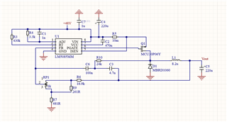
You can see the schematic for this design below.

I've checked all connections, I've tested this with an eload, everywhere from 10 kO to 100 O, and it's not switching at all. I tried replacing the IC, and I even tried replicating the design on page 17 of the datasheet, replacing R3 with a 100 kO resistor, R4 with a 2.2 kO resistor, R10 with a 68 kO resistor, and C3 with a 2.2 nF capacitor.

Nothing changes the output. I'm kind of at my wits end here and would appreciate any assistance. At this point, I don't care about current regulation or current limit, I just want to see some voltage regulation.

  • Hello Alexander,

    It looks like your attempt to run open look is presenting a voltage at the FB node, greater than the reference voltage and as such the device is running at 100% duty cycle.  Can you check the voltage at the FB confirm, please reopen thread if this does not resolve. Thanks.  

    Hope this helps.

    David.

  • Hi David,

    That is correct. The voltage at the FB pin is greater than 1.25 V, but I'm not operating this in an open loop. There is just a potentiometer as a part of the feedback path. If Vfb > 1.25, shouldn't the controller turn the PMOS off?

  • Sorry for the confusion Alexander, 

    The PGATE high means that the PFET is off.  You are setting voltage at FB pin to VREF and the device is doing what it is supposed to do by turning off the HS MOSFET.

    Can you make the PGATE go low by reducing the voltage at the FB node?

    Thanks.

    David.

  • If the PMOS is off, then how come Vout is roughly equal to Vin?

  • Hello Alexander,

    You mentioned the Pgate remained "high" and I assumed that the P- CH mosfet is off.  If VIN=VOUT then PGate would typically be low.   If PGATE is actually high (Pgate = VIN) and VIN = VOUT, then the FET is short circuit.

    David.

  • That would indicate that it's behaving like a short. I just checked Rds, and it's on the order of several megaohms. I also checked the markings on the part, and they are correct.

  • I measured Pgate = 48.19 V. Vin = 48.2

  • I also measured Rdg and Rsg, and they were several MO

  • Hello Alexander,

    If Vout = Vin and PGATE is high, i.e. at Vin, and the FET has not failed and wired in correctly, you must have another path of current from Vin to Vout.

    Hope this helps,

    David.

  • It turns out that the source and the drain were inverted. That sort of solved the problem... We're able to regulate the voltage to a certain degree. As I mentioned, there is a potentiometer in the feedback path to adjust Vout between 32 V and 45.7 V. Things seem to work well at 32 V and as we increase the voltage to 38 V, but once we exceed 38 V, Vout drops to 33 V and stays there.

    I probed Vfb in order to get a handle of this. At the lower values of Vout, Vfb = 1.25 V as expected, but once we exceed 38 V, it drops down to 0.9 V and stays there.

    I've made three peculiar observations:

    1) If I probe the transistor gate signal with an oscilloscope probe, we're able to get up to 42 V.

    2) The circuit behaves differently if we start at Vout_min and rotate the potentiometer towards Vout_max than if we start at Vout_max and rotate the potentiometer towards Vout_min. I've already described the former case. In the latter case, Vout stays around 33 V the whole time.

    3) When the circuit is unpowered, and I measure the resistance between the potentiometer wiper and one of its other terminals, and even without adjusting the potentiometer, the measured resistance would slowly drop. This is similar to what I see when measuring the resistance of a capacitor, but much slower.

  • Hello Alexander,

    It sounds like you have a resistive load and you are hitting current limit, this would explain what you are seeing.  Please try to increase the current limit level or you can increase Rload, (decrease Iout) and see if this resolves your issues?

    Hope this helps.

    David.

  • Alas, the load is practically open. That would also not explain the asymmetry between how the circuit behaves when adjusting the potentiometer from high to low versus low to high. It would also not explain why I can get to 42 V if I'm probing the transistor gate with an oscilloscope probe.

  • Although I will note that I did test it with an ELoad. At low output voltages, it performed well up to 500 mA (I didn't test further).

  • Hello Alexander, 

    The asymmetry is probably not related.  Are you sure that the devices FB pin did not see greater than 7V when you were trying to get the device to work with the MOSFET in back to front?  If FB>7V the device will be damaged.  not sure what you did differently from the above schematic.

    Also, please can you probe the gate voltage before, during and after the point of  question? 

    Thanks, 

    David.

  • Hi David,

    We replace the device, so I can guarantee that it never saw more than 7 V. I see very little at the gate. It's pretty much just 48 V. It doesn't seem as though there is any switching.

    I will note that our technician installed the big electrolytic output capacitor backwards (ie. wrong polarity). We definitely saw switching at the gate before reversing it to the correct polarity. Normally capacitors with reversed polarity are only a danger to themselves. Is it possible that it may have damaged the FET?

  • Not sure Alexander, 

    Edited.

    However, I am almost certain something appears to be damaged if you don't see any switching regardless of VIN and something has changed during experimentation.  I would replace all of the semiconductors...

    David.

  • Hi David,

    I'll ask our technicians to do that today.

    Thank you!

  • Hello Alexander, 

    Feel free to reopen thread if issue persists.

    Thanks,

    David.

  • Hi David,

    Our technicians replaced the transistor, the diode and the regulator, and we're still seeing exactly the same problem. I don't see any switching, and yet there is a substantial voltage drop across the FET.

    I probed the pins at both extremes of the potentiometer. Everything seemed pretty good. Here is what I found:

            "Low"       "High"

    ADJ: 48.06      48.07

    RT:   1.752       1.745

    FB:   1.248       0.920

    ISEN 48.21      48.22

    PGATE: 48.21  48.20

    VCC: 40.42      40.42

    VDD: 48.22      48.22

    Vout: 32.11       34.07

    I did notice one strange artifact. Throughout most of the power side of the device (PGATE, VDD, VIN, ISEN, .etc) I saw periodic impulses. The frequency of these impulses was dependent on the position of the potentiometer and varied between 400 Hz and 800 Hz (relatively low frequency). Of course, I checked my power supply, but it wasn't present when not connected to the PCB.

    Thank you!

  • Problem solved! Something was soldered to C7 (bypass capacitor for Vin) that was definitely not the 1 uF capacitor that it was supposed to be. I have no idea what it was but right now, I don't care. We're able to get our full and expected range.

  • Oh, that great news Alexander.

    Glad you were able to resolve the issue.

    David.