


Hello Everyone,
I am designing BMS for 48V 100Ah battery pack. It must able conduct 100Amps current conntinuously. I am confused about discharge FET drive circuit. There is 2 different circuit. First one just used gate resistor and other one uses pmos for gate drive. What is the difference for usage? Why do we need to pmos to drive discharge FETs. Reference schematics are in the below.

Gate Resistors
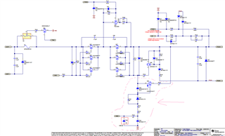
PMOS
Thank You,
