This thread has been locked.

If you have a related question, please click the "Ask a related question" button in the top right corner. The newly created question will be automatically linked to this question.

TPS92641: Flicker Problems on TPS02641 using external Shunt FET Dimming

Part Number: TPS92641
Other Parts Discussed in Thread: TIDA-01095, TIDA-080008

Hi,

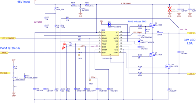
we have an issue with a TPS92641 LED driver. The schematic is this:

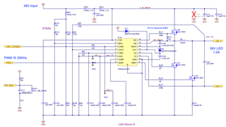
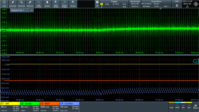
Supply Voltage is 48V, LED String Voltage is 38V, LED Current is 1.5A

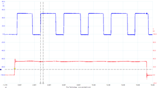
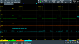
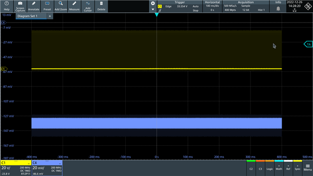
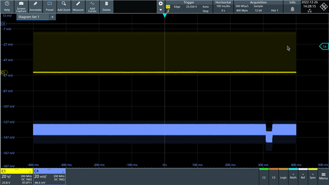
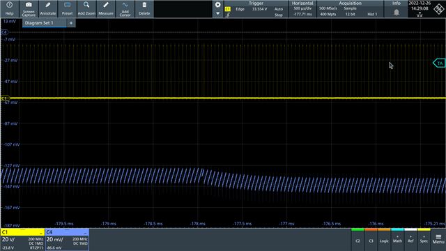
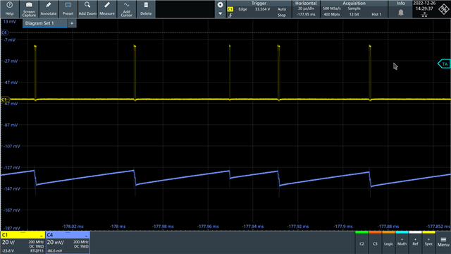
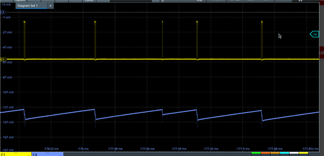
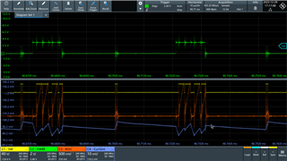
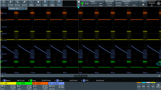
We have discovered flicker problems which occur at specific duty cycles when using the Shunt FET dimming. Our PWM frequency is 20KHz. When we linearly go through the entire dimming range we can observer multiple duty cycle settings which produce visible flicker (e.g. 2-4 points from 0-100%, for example 50%, 71%).

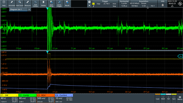
We have narrowed it down to the drivers current regulation which seems to oscillate at certain settings. We have tried to change a lot of thing already, but nothing really did solve the issue. The only change that happens is that the dimming level where it happens moved to different values.

Our tests so far:

- Higher value for CS resistor R115 (22k)
- Smaller inductor (68uH, 100uH)
- Bigger Capacitor for Comp C89 (1uF)
- Different driver frequencies up to 600KHz
- Different Output Capacitor C103 (limited options as Q11 gets too hot, if value goes beyond a few dozen nF)
- Bigger Sense resistor R111 (150mR - slightly reduces current already)
- Slowing down of FET transistors by changing R108, R113

Looking forward to your help as we are running out of options to save this design.

Best regards,
Thomas

  • hello Thomas

    I would like to require some waveforms of SW, HG, LED string voltage, voltage across R111 under flicker condition.

    BTW, the boot cap C104 looks quite small, you may try to increase it to 0.22uF and see any difference.

  • Hi Mason,

    we have increased the boot capacitor. Not sure why it was set to 4,7nF, but I guess it clearly is too small. Increasing the boot capacitor did improve the overall dimming, but did not really solve the flicker issue.

    Here are 2 pictures from the SW Pin:

    We observed that the first gap sometimes has different size, but we don't know if that is the issue.

    Here is a picture from the HG Output (measured between 100R and Gate):

    Here is a picture from CS, but taken from an older measurement where the driver was set to 800mA and having a small shunt resistor. Currently shunt resistor is bigger and the driver is set to 1.5A. We will try to make a better picture in the next days.

    Overall it is really hard to measure the flicker as it is very low frequency, quite random and quite low in amplitude. Birghtness varies only by ca. 2-3%, but with the low frequency it is just enough to be visible and the use case for this product forbids any visible flicker.

    Best regards,
    Thomas

  • I should add that we have put a 100nF on top of the 4,7nF boot strap capacitor - not 220nF. Is that big enough or do we need more? The Mosfet have very low gate capacitance.

  • Hi Thomas,

    Mason is out of office due to sick leave. He'll reply to your question once coming back.

    Sorry for the inconvenience and thanks for your patience.

    BR

    Patrick

  • Hi Patrick,

    thanks for letting us know. We will wait patiently and try getting more info in the mean time.

    We have one more questions about the operation of the chip: The differential amplifier switches inputs (CS and iAdj) to avoid any offset. How does this mechanism work when the Shunt FET is shorting the output? Is it switching inputs with the frequency of the SW pulses? If so then this switching might be very slow and thus offsets might become visible.

  • Hi Mason, please check the attached screenshot. We have used a new scope now which may give us some clues what is happening. I have drawn a few blue arrorows. When we let the scope run we can see that the chip is turning on SW immediately when the Shunt FET is closing. But what changes a lot on each cycle is the number of times the SW pin is triggered afterwards. It might be that it just charges the coil once, twice of up to 6 or 7 times with very close timing. Then for a long time nothing happens until PWM starts over again. We believe that this might be what is causing our flicker.

  • We figured that putting the high-impedance probe from the oscilloscope on the CS pin was causing the extra spikes at the end. It seems that CS is very sensitive to noise. Maybe this is our real issue.

    What is the purpose of R115? In the datasheet there is not much information about this resistor. I remember in a demo application on the website it was set much higher than this.

    We also added 1nF on the CS pin to GND to reduce EMC, but this doesn't seem to be enough to stop the flickering. On the layout Chip Signal GND and the GND of the sense resistor are on a polgyon close to each other. So these should have good connection.

    Best regards,
    Thomas

  • Hi again,

    meanwhile we have been investigating this issue further and I believe we might have found the issue. Please see below:

    Setting PWM to 0% we get this waveform. Yellow is the SW input, Blue is the current running through the inductor measured with a 50MHz current probe (I extended the leads of the inductor so I could attach it). This so far looks good. The timebase is very long and if you zoom in you would see the sawtooth on the power.

    Running the trigger manually multiple times I sometimes get other waveforms:

    or

    or other variants that all do the same: The power level of the inductor is shifting by ca. 100mA for several ms up to tens of ms. Now zooming in:

    further

    and further

    and even further:

    It seems that the chip is regularly double pulsing to keep the inductor charged, but only from time to time there seems to be just a single pulse. This pulse is the point where the current shifts until the next single-pulse even when it shifts back.

    Our assumption is that the offset compensation of the internal opamp is triggered by current regulator pulse:

    So as long as we always get double pulses the offset compensation doesn't work as it basically stays in always the same state. Now when a single pulse occurs the inputs are toggled and then again persists for as long as there are double pulses. On the next single pulse it shifts back to the initial state.

    There is no information in the datasheet about how "clk1" is working - could you elaborate on this? To me this appears to be a design issue of the chip.

    Btw: Looking at iAdj and Comp with the scope show a flat line with only some switching noise from the Mosfets. They seem to be pretty stable.

  • Now what happens when PWM is active. Knowing what to look for there seems to be the same issue happening here:

    PWM is at ca. 30% (orange). Current glitches visible when zoomed out a lot:

    Zooming in:

    and further:

    Scrolling through the data I can see that this PWM setting normally creates exactly 6 pulses on the SW pin. In between again there are usually double pulses when PWM is off. So all even numbers not changing the polarity of the offset compensation in the chip (my assumption).

    Now from time to time again there is only a single pulse happening in between which is the trigger for a current shift on the output in the size of 100mA. Frequency is low (single digit Hz) and duration is anything from a few ms to tens of ms.

    This matches the flicker we can see by eye on the wall and it also explains why it only happens on certain PWM values as it only happens if the selected PWM value generates even pulses as otherwise with every PWM cycle the current would be shifiting.

    Looking forward to your reply.

    Best regards,
    Thomas

  • When looking at the graphs again I just realized I might have put the current sensor the wrong way on the cable. The blue curve (Current) should be inverted as obviously the current goes up when the SW output is high and falling in between the pulses.

  • hello Thomas

    sorry for the delay on this thread.

    1. I've gone through the schematic again and wonder why VCC is additionally tied to 12V with D11 

    2. based on the result with PWM 0%(means no shunt dimming), there is still the current oscillation. Did you measure the inductor current by a sense resistor and what is the ratio that I can get the current value?

    3. Based on #2, I would like to check the condition without shunt dimming first. can you monitor voltages of comp pin and RON pin again together with SW and inductor current below. You can use a small scale since the variation can be small.

  • Hi Mason,

    see my replies below:

    1. This supply is meant to bypass the internal LDO that powers the Mosfets. In the first design we didn't have this and the TPS92641 got quite hot as the internal LDO had to dissipate quite some heat. Our PCB design doesn't allow to dissipate that much heat and this solution cools down the chip pretty well.

    2. I removed the Inductor from the board and added 2 short leads each 3-4 cm in length. I have used an Agilent N2782B 50MHz current probe to measure the current without the need to add an extra shunt resistor. That is also why on some pictures the current was inverted - I attached the probe in the wrong way. The probe generates 0,1V/A.

    3. I will masure ROn and send you pictures asap. I did measure Comp before, but I could only see a flat line with switching noise on top. I will make a picture together with ROn.

    Btw: I am still interested to hear what the purpose of R115 is? In the demo designs on the TI website the value for this resistor has quite different values (475R on TIDA-01095 vs. TIDA-080008 (49,9 with a C vs. GND - most likely supposed to be a low pass filter on CS). Does it make sense to put a ferrite bead here to reduce noise on CS?

  • Here are the requested pictures:

    Yellow: SW
    Green: Comp
    Red: ROn
    Blue: Current

    ROn only shows a bit of switching noise. Comp shows more switching noise, but apart from that seems flat. I have put it into the top window as otherwise the switching noise would overlay the data on the other curves.

    Zooming out again and triggering on the problem again it becomes visible that COMP slightly changes together with the current change:

    In the middle of the graph you can see the "1 SW Pulse" happening again after which the Chopper amp inverts and the DC offset of the opamp increases the level of COMP and thus the level of current on the inductor.

    To me this looks like a design issue on the chip as whenever the output is shunted the pulses on SW become so slow that the chopper amp doesn't cycle fast enough anymore and the averaging of both inputs that is needed to cancel the inherent DC offset isn't working anymore.

    Maybe this would be better, if the chip would only create one single pulse and not the double pulses when it is shunted. Could this be helping?

  • hello Thomas

    1. thanks for your explanation on this action.

    2. then for channel4, why it shows this is a voltage signal? I had thought you measure the voltage on a shunt resistor.

    3. Pls refer to 7.3.4,  R115 (RF) together with Roff work for true zero application.  

    Normally when user give the zero current command by giving Viadj=0V, there is still current flowing through LED due to the structure of synchronous buck converter. So RF and Roff are configured to bypass this current since LEDs are not supposed to light if user demand zero current.

    4. actually there is not much detail on chopper OTA that can be traced back to. From the current result, the operations for both PWM on and off are abnormal. when shut dimming off, the inductor current is supposed to regulated at a stable state which means peak value and valley value of inductor current should not vary. when shut dimming on, output voltage is pulled down to zero and HG pulse will be fixed at a min. on time while in the result it is missing for some cycles.

    can you try to add 1nF capacitor at VOUT pin, this is the voltage feedback for the internal on-timer. At the same time, do you have a EVM board that can do comparison test since currently I am home office due to covid?

  • hi thomas

    will it make any difference with higher input voltage or lower LED string voltage? since 48V-38V will have a large duty cycle and min. off time could be triggered and this may lead to abnormal inductor current during shunt dimming off period.

  • Hi Mason,

    thanks for your reply. Here are my responses:

    1. The Agilent current sensor outputs a voltage proportional to the measured current. It has its own electronics and amplifier. The oscilloscope doesn't know it is a current measurement device and thus thinks it is a normal probe that delivers a voltage.

    2. In your graph the pulse is not missing, but it happens late - most likely due to overcurrent from the cycle before. It can be seen just starting when PWM turns on the light:

    3. I can try the higher supply voltage and the 1nF capacitor this afternoon. I will have to go to the office an pick a lab supply and some capacitors.

    Best regards,
    Thomas

  • Forgot to ask: Does it make sense to add the ROff in our case? We don't do analog dimming, so maybe it is not necessary?

  • Hi Mason,

    increasing the supply voltage to 60V makes the current stable when the PWM FET is turned on:

    Looking closer reveals that in this case we always get double pulses and no more single pulses:

    This appears stable, but in essence the chopper amp still rests in one single state and we got an offset to the current - it just doesn't flip due to missing single pulses.

    When applying PWM at 60V supply voltage things start to fall apart again in the same way as before:

    However I need to select different PWM values before to make it flicker. Higher PWM values appear to be more stable due to the fact that there are no more pulses during the dead time. Most likely the inductor gets charged quite well with 60V and if dead time is short enough there is no need to charge it again when the PWM FET is closed.

    I believe we would solve the issue, if we can get rid of the double-pulses during the time where the Shunt FET is closed. Then we would toggle the chopper amp with each PWM cycle and get a stable average current on COMP.

    I will check the 1nF on VOut next.

  • Hi again,

    when PWM is running I noticed kind of a sawtooth waveform on ROn during the time when PWM is on (shunt fet open). It doesn't matter whether if we use 48V or 60V supply voltage.

    Is that expected behavior?

  • hi Thomas

    1. the sawtooth waveform is the expected behavior. R125+R123 and C85 is part of the internal on-timer. Every time the inductor current drops during switching off time and reaches comp voltage level, the voltage on C85 is released and charged again from zero until a constant time and this time equals to switching on time. can you check the switching on time? normally it should follow formula below, which is ~2,37us under your input/output voltage and Ron, Con setting.

    2. from your description, the current probe is 0.1V/A. In the waveform, it does not even reach 100mV (1A) while normally average of inductor current should reach 150mV (1.5A). So if the sense voltage is below IADJ/10, the comp voltage should always increase to pull the current up. So can you monitor the voltage of CS?

    pls increase the duty cycle of PWM to like 80% to see more details. BTW, is the PWM (channel 2) directly applied on Q11 or it is inverted? my understanding is that with shunt PWM control signal on, Q11 is turned on and Vout is shorted.

    3. At the very beginning, you mentioned you have tried increase output capacitor? any improvement with 0.1uF capacitor? with a too small capacitor like 1nF may lead to a high bandwidth and limited phase margin of the system. 

  • Hi Mason,

    here are the requested measurements with 1nF on the VOut pin. Maybe this capacitor is too big?

    I reduced it to 27pF for testing:

    This looks ok as long as there are enough pulses. If PWM gets shorter then the first pulse still seems distorted:

    Maybe 27pF is still too big?

    Regarding your questions:
    - Right now for testing there is no output capacitor. I can put one for testing.

    -To be honest I haven't looked at the absolute voltage from the current probe - just the ripple size. It has a potentiometer to set the 0 position. I will need to check it to see, if I can get a good look at the absolute current. Should be possible I think.

    For the last measurement I used a second PCB as it appears I destroyed the other one that I was using for testing  yesterday when I have added the 1nF capacitor on Vout. The first PCB had all channels set to 1.5A, but the second PCB might have been set to 0,8A on that particular channel for a test. So that could be why it didn't reach 150mV.

  • Hi  Mason,

    I made some progress during the last days and I believe I got rid of the double-pulses on the SW output and thus have solved the chopper amp switching problem that led to flickering. I don't really know how the internal control loop behaves when the Shunt is closed, but I guessed that maybe the "constant on time" pulse just wasn't enough to charge the inductor for where the chip wants the current to be and thus creates a second pulse directly after the first. I have reduced the size of the inductor to 68uH and increased switching speed to 640KHz to get to a similar ripple as before which seems to have done the trick.

    I also tried different sizes of output capacitors (1nF, 10nF, 100nF). 100nF already seems to much and significantly reduces low-end resolution. 10nF seems ok and now I can see that the overall regulation seems to be much more stable. This also helps reduce noise on Vout - so I left out the additional capacitor that you had recommended for Vout.

    So hopefully the initial problem is solved (we will do more tests in the coming week).

    However I now run into a new problem (I guess it would be to easy otherwise) which I would describe as "steppyness": Tiny amounts of change on the current can create bigger steps in output current. It seems to be a repetitive problem - it feels like intermodulation and definitely has to do with timing of PWM and the switching cycles of the chip.

    What happens is the further you increase PWM the bigger an overshoot at the turn-off point of the PWM appears. It increases until a certain point and then when PWM is increased just a liitle bit more (really fractions of % - not visible to the eye) it jumps back to zero overshoot and the cycle repeats again when PWM again increased. The overall dimming curve thus has visible steps and is not smooth.

    I have made 2 screenshots showing before/after such a jump:

    No overshoot on turn off:

    Zooming in:

    Slightly different PWM with maximum overshoot:

    Zooming in again:

    Normally I wouldn't care about a bit of overshoot happening during the dark time, but it seems that this also changes the average current that flows through the LED when it is on by ca. 70-80mA - enough to be visible as a step in brightness.

    I added some measurements on the bottom of the screenshot. It seems to me that the average current is always stable at 1.5A, but this seems to include the current during dark time (shunt fet closed) and due to the overshoot there the average current during on time is dropping which creates the step in output brightness.

    Do you have any idea how to counter this problem?

    Best regards,
    Thomas

  • hello Thomas

    From your waveform result, looks like there is a delay between PWM off and switching off. Is it a fixed time? The delayed switching on time leads to a high current ramp since during this period of time Vo=0, inductor current ramp rate equals to ton*Vin/L while normally it is ton* (Vin-Vo)/L. If the SW is low when PWM off, I suppose there will not be such high current ramp, is that correct?

    I agree that this should have something to do with PWM frequency, duty cycle, switching frequency, duty cycle. Do you mind checking the actions:

    1. increase switching frequency, currently it is 640kHz?

    2.  decrease comp capacitor from 470nF to like 100nF

  • Hi Mason,

    yes this is what we have figured as well. Sometimes the chip doesn't turn off the highside FET fast enough. The weird thing is that this does not seem to be a hardware delay of the FET as this time it not fixed. The chip is perfectly capable to turn of together with the PWM. There are PWM values where it turns off allways good, some others where it always overshoots and some values in between where both can happen to a different degree. It all depends on when the PWM turns off in relation to the SW pulses. So increasing the PWM step by step will gradually lead to more overshoot until it jumps back to no overshoot (think of kind of a sawtooth function). At the edge where it is jumping back it might do so with some jitter - thus some pulses there are good and some are not.

    When it overshoots then it does so, because the SW pulse it too long. Sometimes it is the last SW pulse of the PWM cycle which is prolonged and sometimes there seems to happen the first dead-time pulse (DCM mode) immediately after the PWM has stopped moving current too high.

    We have changed a lot of values to see, if this changes (COMP capacitor, inductor size, switchting frequency, gate resistor of FETs, more filtering on VOut/CS), but the behavior is consistent. We believe this is somehow caused by the logic inside the chip during DCM mode.

    Could you tell how exactly the chip regulates current during DCM mode? Is it still doing valley control? From what I understand is that in DCM mode it only performs fixed on-time cycles of ca. 250ns with varying dead-time in between. But when does it create a pulse? It doesn't look like it does the same regulation algorithm as when it is in CCM mode.

    Best regards,
    Thomas

  • hi Thomas

    I suppose here "DCM" means the period of time when PWM is off since normally we say it enters DCM when inductor current drops to zero.

    My understanding on the control principle when PWM off is that on time is a fixed min. value and the time with a pulse is when inductor current drops to reach comp voltage which is similar to valley control. So for the condition with large overshoot, there is even no pulse as the inductor current never reaches comp voltage during dropping.

  • Yes, that explains what it happening during PWM off time, but I still don't understand why the average current during PWM on sometimes drops - depending on the overshoot situation that results from certain PWM values. I can see that when I run through the available PWM values that there are certain seetings where the overshoot after PWM off gets higher and at the same time the average current during PWM on is dropping which causes visible flicker and steppiness.

  • hello Thomas

    sorry for the delay. Yes, I also observed that and normally the behavior at PWM off should not have a influence on the stable operation when PWM on. I suspect the comp voltage with high overshoot is lower than that of normal condition. My analysis is that when there is an overshoot during PWM off (shunt Fet on), the comp voltage drops since current is higher than reference. Then when PWM on(Shunt Fet off), there is not enough time for the comp voltage to be regulated to a normal value since the time period is short and system loop cannot response. will it be different with larger on time that comp can slowly back to normal value? 

  • Hi Mason,

    we have observed that a lower PWM Frequency reduces this problem. Setting PWM for example to 5KHz avoids the problem completely, but this is not really a satisfactory result as our customer is targeting 20KHz for his application.

    Why does it sometimes take so long for the chip to turn off the SW output when PWM goes low? In the graphs you an see that the last SW pulse persists for a few hundred ns after PWM goes low. The pulse also is longer than minimum on time. So why doesn't it turn off?

    It is a cyclic problem: If we increase PWM further and further the overshoot becomes less and less (PWM probably matching "better" the SW pulses) until it jumps back to full overshoot again. Further increase then again reduces the overshoot again and the problem repeats. Much like a saw tooth graph.

  • hi thomas

    My understanding is that the delay is coming from system response speed. Let me discuss this internally and get back to you tomorrow.

  • hi thomas

    This is really coming from the internal control logic that the device senses both PWM on period and PWM off period which leads to a lower comp voltage value. this finally get a lower current during LED on. Actually we do not have a solution to totally solve this issue. One thing that may have some benefits is to increase the inductor to lower the ripple. Actually we have a new device which is under sample stage supporting 2A and 20kHz fast dimming with quite good current linearity and dimming ratio. If it is still in the design window, I can share some information with you by mail if needed.

  • hello Thomas

    sorry for the late reply. to eliminate the delay time, maybe we can try to add a PWM signal at UDIM pin. The logic is that the moment shunt FET start conducting, we pull UDIM down, this will force off state of gate signal. can you help try this action?

  • Hi Mason,

    we have ordered new driver PCBs with some additional changes to see where we stand now. We especially have added a series resistor to the shunt FET as suggested in another thread in this Forum.

    The new PCB does not offer to pull UDIM low, but I believe we had tested this and I also think that the UDIM pin is quite slow in its reaction time. Is that true?

  • hi Thomas

    so you have already tried apply PWM signals both on UDIM and SDIM at the same time? what I mean here is not simply using UDIM for PWM dimming. UDIM acts as enable of TPS92641, pull UDIM down will directly disable gate driver. So I think pull-down reaction time should be fast.