This thread has been locked.

If you have a related question, please click the "Ask a related question" button in the top right corner. The newly created question will be automatically linked to this question.

TPS5432: EMI - electromagnetic radiation

Part Number: TPS5432

hi,
I've created a printed circuit that implements this schematich : LINK to schematic portion

I' ve measure by a loop antenna, over induttance L1, this emission: LINK to image of emissions spectrogram

Can you tell me if you have had similar problems? if you have found solutions to reduce emissions?

  • Hello Stefano,

    Which switching frequency this circuit has? 700kHz if I am not wrong because that is what device has. Can you please share the Layout also?

    Thanks,

    Farheen

  • can see at this LINK to layout

    the PCB dimention is 15x12.7mm
    the PCB is a single layet with copper only on top layer

    this circuit are plugger and solded over another circuit see LINK do adapter

  • Hello Stefano,

    Thank you for sharing the layout.

    There are multiple things that I noticed in the layout and schematic:

    As this looks like from switching frequency, because the highest peak you see at around 666kHz,So it can be related to input capacitor and input loop inductance. Because this is the area that determines the amount of energy stores in this band. So my first suggestion is to have a better connection of Cin to Vin. Placing the Cin caps near to IC Vin pin as close as possible.

    Another thing, it is a single layer board as you said. Having a multilayer board also helps then you have a separate GND plane which gives the better return path for the current. 

    Page 8 of this app note (https://www.ti.com/lit/an/snva886/snva886.pdf) explains this in detail.

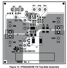
    This the recommended layout where you can see C1 and C2 are input capacitors and how they are placed to minimize the high energy loop area.

    Thanks,

    Farheen

  • in our circuit we have 2x 10uF in 0805 case, we can tray to use 2x22 uF   

    GRT21BR61C226ME13L

    Or also 2x47uF

    0805ZD476MAT2A

    we try and come back to you with the results

  • Hi Stefano,

    Yes, that can also help to improve the results. 

    Thanks,

    Farheen

  • Hi Farheen,

    I tried to add two 22uF ceramic capacitors in parallel to the two 10uF already present, 

    But I didn't see any difference, as you can see from the picture where track A (yellow) is read before the edit and track B (purple) after the edit.

  • Hello Stefano,

    Thanks for the update! What other reason I can see is that it can be due to bad layout. 

    As I said in my comments before:

    "As this looks like from switching frequency, because the highest peak you see at around 666kHz,So it can be related to input capacitor and input loop inductance. Because this is the area that determines the amount of energy stores in this band. So my first suggestion is to have a better connection of Cin to Vin. Placing the Cin caps near to IC Vin pin as close as possible.

    Another thing, it is a single layer board as you said. Having a multilayer board also helps then you have a separate GND plane which gives the better return path for the current"

    Thanks and Best Regards,

    Farheen

  • ok Farheen,
    when we have to redo the PCB we will plan a layout as similar as possible to the one you indicated. Now I was looking for a solution with the PCB already produced.
    But if you say there is nothing to do, we will evaluate the improvement, on the next PCB version.

    Thanks for the support.

  • Hey Stefano,

    Thank you. Because for now I see that Layout is the office option because increasing the caps did not help .

    Thanks,

    Farheen