This thread has been locked.

If you have a related question, please click the "Ask a related question" button in the top right corner. The newly created question will be automatically linked to this question.

CSD25402Q3A: SOA Confirmation

Part Number: CSD25402Q3A
Other Parts Discussed in Thread: BQ25713

Hello TI,

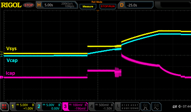
Just wanted to confirm some numbers for the SOA with this pfet.  We are using the bq25713 to charge a supercap and have copied the EVM implementation with a difference of using a 2mOhm sense resistor on the batfet for faster charge up times.  Our charge up time is about 22 seconds.  During initial charge up when the supercap is depleted it must pass through the saturation region of the FET as it charges up to reach vsys which I set to 3 volts.  Once it reaches vsys I then charge it up to 10 volts.  Looking through the data for the current given by the BQ I made some calculations with regards to power and SOA and wanted to have confirmation that we are not exceeding the ratings of the PFET.  

Exporting that data I calculated the power drop across the pfet:

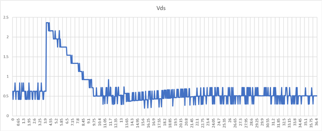
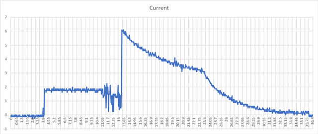
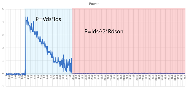
Using these numbers I get a max power at initial charge up when Vds=2.36 and Ids=1.865 amps which gives 4.41 watts.  This number is below the red line for DC in the safe operating area however it exceeds the first maximum power rating on the datasheet.  Do these calculated figures look correct?

  • Hello Walter,

    Thanks for the inquiry. I don't believe that your conditions violate SOA for the FET. The "DC" curve in the SOA graph is based on testing devices to failure at 100ms pulse width. TI considers any pulse width ≥ 100ms to be DC and derates the failure current by 30% for the datasheet curves. For ~2A drain current, the device can support ~12V drain-to-source voltage. However, as you point out, the power dissipation is relatively high especially at the start of charging the supercap and the concern would be exceeding Tjmax of the FET. The maximum power dissipation is calculated assuming Rθja = 45°C/W, Ta = 25°C and Tjmax = 150°C as explained in the blog at the link below. This number will change with Ta (reduced at higher ambient) and Rθja (increased at lower thermal resistance). My approach would be to average the power dissipation over the initial charging period until the FET is fully on. Rθja is measured on a standard, single layer board with 2 oz. copper as shown in the datasheet. The actual performance is very dependent on your PCB layout and stackup. Have you done any thermal measurements during charging to see how hot the FET is getting? The 3.3x3.3mm SON package is our best thermal package for PFET. We don't make any PFETs in a larger/lower thermal resistance package. I hope this helps. Let me know if you have any additional questions.

    The second link is to a blog explaining how TI tests and specs SOA in the FET datasheet.

    https://e2e.ti.com/blogs_/b/powerhouse/posts/understanding-mosfet-data-sheets-part-3

    https://e2e.ti.com/blogs_/b/powerhouse/posts/understanding-mosfet-data-sheets-part-2-safe-operating-area-soa-graph

    Best Regards,

    John Wallace

    TI FET Applications