This thread has been locked.

If you have a related question, please click the "Ask a related question" button in the top right corner. The newly created question will be automatically linked to this question.

TPS62065: work abnormal when the temperature in -30℃

Part Number: TPS62065

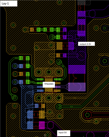
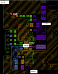
Problem:  The temperature is -30℃, we switch the unit power on, the TPS62065's output voltage is abnormal, the wave and circuit as below:
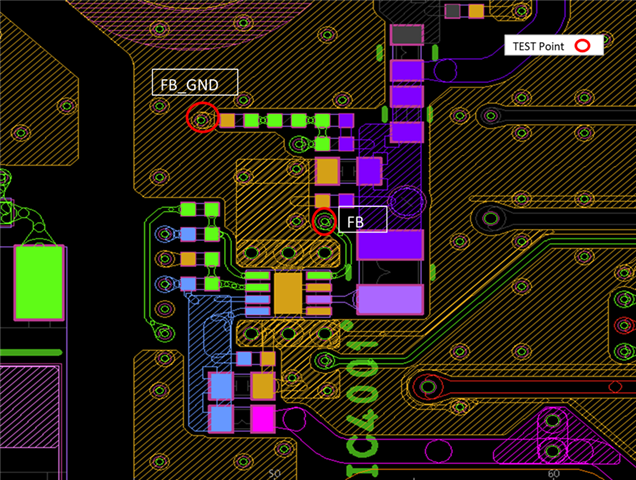
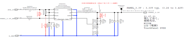
the circuit:

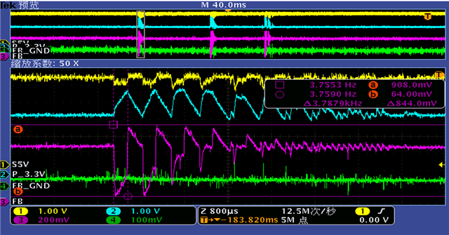
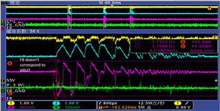
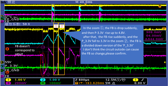
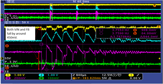
the wave when abnormal:  

pink is the the output (3.3V)

yellow is the input (5V)

blue is the enable signal for TPS62065

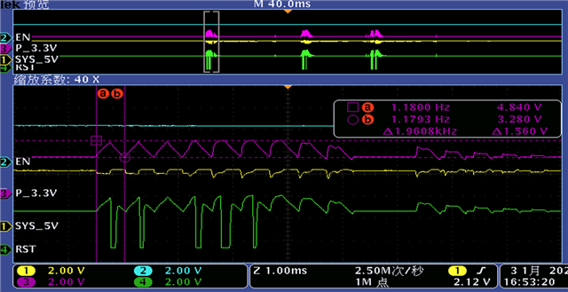
please check and help analyze why  the output voltage up to 4.92V ,and the output seam not be stable.

we have check the phase margin , the result is OK.

and the defect rate is low but the voltage of 4.92V may demage the device.

  • ADD information : the current is about 400mA when it work .

  • Hi Lin,

    Thanks for the information you provided so far. Could you help provide the below info too: 

    1. Is the problem only at -30C? Does it work fine at room temp?
    2. Is there some load transient event that triggers the problem?
    3. Do you also see this issue while operating in PFM mode with Mode connected to GND?
    4. Can you please share the layout of the converter as well? 
    5. You mentioned the defect rate is low. What percentage of tested converters show this?

    Best regards,

    Varun

  • Is the problem only at -30C? Does it work fine at room temp?
    -> we only find the problem in -30C, and the defect rate is low ,so I don't know is it OK at other temp.
    Is there some load transient event that triggers the problem?
    -> the load device is MCU , and TP IC , the current have not a big change.
    but the input 5V have a voltage change. you can see the wave.
    Do you also see this issue while operating in PFM mode with Mode connected to GND?
    -> no, we only check it in PWM mode.
    Can you please share the layout of the converter as well?
    ->the picture as below, 
    You mentioned the defect rate is low. What percentage of tested converters show this?
    ->we quality department check that defect rate is 1/5(POWER ON/OFF) at first.
    but when we want to check the wave ,we find the defect rate is low, about 1 time a day.

    if you have any question , please let me know.

  • Hi Lin,

    On the layout, the FB GND should be connected to the AGND and not the GND plane/ Power PAD. There could be more GND noise from switching in the feedback loop if the FB GND is connected to the power PAD instead of the AGND. The GND noise in the feedback loop could be a reason why you see this overshoot in VOUT. 

    Please check section 11.1 and 11.2 of the datasheet.

    Is it possible for you to try some manual board modification to test this out- cut the connection of R4007 to the GND plane and use a wire to connect it to the AGND pin?

    Could you also let me know what is the end equipment for this project?

    Best regards,

    Varun

  • Is it possible for you to try some manual board modification to test this out- cut the connection of R4007 to the GND plane and use a wire to connect it to the AGND pin?

    Could you also let me know what is the end equipment for this project?

    you means the noise from vin-5v may affect the FB by GND,

    and the best layout is set R4007 connect to AGND(PIN3) first and then connect to the thermal pad , right ?

    like below picture :  can you share the EVB bord's layout (include top lay and bottom lay)

    This project is a navigation unit for Honda 

  • Hi Lin,

    There is more switching noise (due to discontinuous currents in the input loop) that can couple into the the feedback loop if R4007 is referenced to the PGND instead of AGND.

    The right layout would be to connect R4007 connect to AGND(PIN3). And then connect the PGND and AGND at the thermal pad.

    You can find the EVM layout in this folder https://www.ti.com/tool/TPS62065-67EVM-347.

    Best regards,

    Varun

  • thank you for you imformation ,

    We check the FB pin's wave as below:


    I think the cause may not the noise from GND , please confirm it and share your opinion.

  • Hi Lin,

    On the scope shot, the 'FB' signal shape doesn't correspond to the shape of the 'P_3.3V' signal. Both the signals should have the same shape as the FB is just a divided down version of the 'P_3.3V' signal. It could be the GND noise of the VIN probe is coupling onto the FB probe. Can you disconnect the VIN probe and check? To check the GND noise of the FB loop, you would have to measure between the AGND device pin and the FB GND with preferably a differential probe.

    Best regards,

    Varun

  • Dear Varun John:

    I don't think the FB was effected by Vout(3.3V) 
    you can see the image as below:

      In the zoom ①, the FB is drop suddenly, and P-3.3V  rise up to 4.8V.

      after that,  the FB rise suddenly, and the P_3.3V fall to 3.3V in the zoom ②,  the FB is a divided down version of the 'P_3.3V' 

      I don't think the circuit outside can cause the FB so change,please confirm.


  • Hi Lin,

    The traces between the input cap and the device VIN and GND pins have discontinuous currents that can cause the input cap GND to bounce. There is a chance that this GND bouncing when you measure the VIN signal couples on to the FB probe as well. You see both VIN and FB fall / rise by the same amount in each switching cycle. That's why I had asked to double check this with VIN probe disconnected. You should also use the 'FB_GND' point in the layout pic as the point to connect the FB probe GND connector.

    The FB signal in the IC is just an input pin to an error amplifier. It's purely an external signal that is fed to the IC and there is nothing in the IC that changes it's shape. If you look at your schematics, the FB voltage is a divided down version of the VOUT using resistors R4004, R4006 and R4007. So ideally it should have the same shape as VOUT. Looking at the scope shots it looks like it is the sum of the VOUT shape plus the noise from VIN.

    Inside the IC, the error amplifier compares the external FB signal to the internal reference signal, VREF. The GND reference internally for VREF is AGND. However, if externally the FB is referenced to the PGND instead of  the AGND pin of the IC, there can be more noise in the FB signal. This can cause unexpected switching and regulation behavior of the device.

    Best regards,

    Varun