This thread has been locked.

If you have a related question, please click the "Ask a related question" button in the top right corner. The newly created question will be automatically linked to this question.

LM5118: switching ring on HO pin of LM5118

Part Number: LM5118
Other Parts Discussed in Thread: LM5116

Hi,

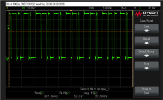
The DC-DC circuits was designed with LM5118, the input voltage range is about 35V-55V, the current load is about 4.2A, I am debugging the board now and found the switching signal has some ring as below waveform shows, the output voltage/current I think is within my expected, noise is somehow worse than my expectation, noise Vp-p is about 2.16V.

My question :

1: how to remove or decrease the switching ring?

2, how to improve the noise

3, I also found the inductor is hot, I measured the temperature of inductor surface under 4A current load, after 30 minutes, the temperature rises to 82 degree C, how to improve this?

The schematic is as below:

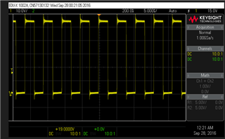
Output voltage noise at 4A current load:

...

Thanks 

Kelvin

  • Hi Lesheng,

    Please add the input voltage/ output voltage condition. And what is the waveform in the first picture?

    Best Regards,

    Feng Ji

  • Input voltage range is 35-55V, and output voltage is 48V, the switching ring is existed at all input voltage range.

  • The first waveform is the switching signal at HO pin of LM5118

  • Hi Lesheng,

    The first waveform is the switching signal at HO pin of LM5118

    Is it HO pin instead of HS pin? What is the input  voltage of the waveform?

    Best Regards,

    Feng Ji

  • Yes, It is HO, NOT  HS, HS is not a switching signal for MOSFET are you familiar with LM5118, if not, would you forward my question to an expert, thanks!

    I have said that the input voltage range from 35V-55V, the switching signal waveform is similar within this input voltage range.

  • I want to know the input voltage when you take the waveform. It is not a range.

    Please describe your question precisly, otherwise it will be diffcult to determine the reason.

  • The switching signal ring existed within voltage range from 35V-55V, it means at any input voltage level of 35-55V, the switching signal ringing waveform is similar, do you understand?

    The noise waveform was recorded at 43V input voltage/4A current load.

  • Do you have any updating for this question?

  • Do you have any updating for this question?

  • Hi Lesheng,

    LM5118 should be in buck-boost mode with Vin=43V and Vout=48V/4A.

    But below waveform seems it still operates in DCM. Are you using 47uH inductor? or the load current is not 4A.

    And where do you put your ground in the below waveform? Or the waveform is AC coupled?

    1: how to remove or decrease the switching ring?

    The ringing is here because you are operating in DCM.

    2, how to improve the noise

    Improving the ripple is a big topic. high ESR of the caps, low capacitance, bad layout...may cause high output ripple. And make sure you are measuring the output ripplein the right way.

    3, I also found the inductor is hot, I measured the temperature of inductor surface under 4A current load, after 30 minutes, the temperature rises to 82 degree C, how to improve this?

    Generally, you should determine whether core loss or winding loss is dominating. If core loss is dominating, you should increase the inductance to reduce the inductor current ripple.

    Best Regards,

    Feng Ji

  • I re-do the testing and record the waveform of HO switching signal at different current load conditions, but I always failed to paste the waveform on this page,

    would you let me know you mail so that I can send you mail?

  • The switching signal waveform I pasted was captured under very light current load 0.5A, it is not 4A.

    The noise waveform was captured under 4A current load.

    Below is a waveform of switching signal of HO I captured under 45V voltage input/4A current load:

    From the waveform you can see the pulse width is changed, some pulses is very narrow, can you explain why the pulse width is different ?

  • Hi Lesheng,

    This narrow and wide pulses are typically a sign that the slope compensation is not set OK.

    Can you please check this components on the RAMP pin.

    You can also use the CALCULATION TOOL

    LM5118/LM25118 Quick Start Component Calculator (Rev. A)

    which can be found on the product page.

    Best regards,

     Stefan

  • Yes, I have been told by somebody else that it is the slope compensation problem, but I really don't how to adjust R/C value combination, would you advise me how to choose a right R value and C value to do debugging?

    I have pasted the schematic, the current R/C VALUE combination is 36.5K/4700pf, would you advise a R/C combination?

    Input Voltage range is 42V-55V, Nominal input voltage is 48V, output voltage is 48V, Maximum Current load is 4.2A, DC-DC frequency is 400Khz

    Thanks

  • Hi Lesheng,

    can you please use the calculation tool mentioned above and put in your design data.

    When sharing it then here in the forum, we can better discuss the component selection.

    Best regards,

     Stefan

  • Hi,

    snvu065a.xlsm

    I have input the design data as I can as attached exel file, actually I don't know how to select design data for step 9- step 15, I guess it may not impact the slope compensation.

    Would you have a review and kindly give your advice for R/C selection?

    Thanks

  • Hi Lesheng,

    thank you for providing the excel sheet.

    A few comments:

    as indicated in the excel calculation please use Cramp 1200pF and Rramp 37k

    It also looks like that the used current sense resistor is quite high - so it can trigger overcurrent when going to max load.

    The Tools suggest 15.09 mOhm but you have used 20mOhm which is almost 25% higher.

    For step 9: do you have a spec for the output voltage ripple? Or what is the unknow data here?

    For step 10: just enter the value from your schematic for the upper resistor on the FB pin - the tool gives you then the lower -> is OK 

    For step 12: when entering the values for the compensation, the bode plot shows that you have set a quite low cross over frequency of 500 - 800Hz.  
    With another compensation a cross over frequency of 4kHz could be reached as well.

    Best regards,

     Stefan

  • "For step 12: when entering the values for the compensation, the bode plot shows that you have set a quite low cross over frequency of 500 - 800Hz.  
    With another compensation a cross over frequency of 4kHz could be reached as well."

    I guess you are talking about step 13 of the calculation tool, actually I didn't input anything for this step, because I don't know how to do it , it is the default value of the tool, not by my inputs.

    what is the problem of low cross over frequency? do I need increase the frequency?

    For the ripple noise, I think 2% of output voltage level is acceptable, for 48V output voltage, the ripple p-p 1V is acceptable.

  • Hi Lesheng,

    if a low cross over frequency is OK for you then it is fine, just wanted to let you know that you have some more margin.

    This influence on how fast the system can respond on load transients.

    Best regards,

     Stefan

  • Hi Lesheng,

    if you would like to learn more about compensation: here is a good report:
    Switch-mode power converter compensatin made easy

    Best regards,

     Stefan

  • Thanks for this document.

  • Hi Lesheng,

    I have not seen an update for the last 26 days, so I assume the questions are/or answered and the issue is solved.
    I close this thread now. If there is still something open reply and the thread will get open again.
    If you have any other question or of the thread gets locked, please open a new one.

    Clicking the Resolved Button also helps us to maintain this forum.

    Best regards,
    Stefan

  • sorry for late reply, actually I have been working for tuning the circuits all the time, but still can't meet my requirement, I have adjusted the compensation loop as you suggested and the switching signal looks good after adjusting, but the load regulation became worse, if I don't change anything the load regulation can meet requirement, but SW signal looks not good, my expectation both are good, SW signal is clean and load regulation is good.

  • Hi Lesheng,

    Is it possible for you to provide oscilloscope screenshots for switch nodes and output voltage (showing the load regulation) for both cases and an exact description which components have been used for which case?

    Thanks and regards,

    Harry

  • Can I communicate with you by mail, there are four DC-DC power supplies on board, two use LM5116, two use LM5118, I found all four DC-DC have one common issue, the SW signal is not perfect, the pulse width is changing, some pulse is very narrow, some pulses looks OK, some pulse is wide. I spent many time to fix this issue, but failed, they look like below pictures:

  • Hi Lesheng,


    You have mentioned that the two LM5116 based converters also show the varying pulse width.
    Can we also please get the following information for the constellation where this is happening:
    VIN, VOUT and IOUT?

    Looking at your schematic, I have a question on it: Except for C16 and C28, are you using any ceramic capacitors on the input and output of the converters?
    Or are C93, C14 and C154 the only input and output capacitors?

    Please clarify.

    Best regards,
    Harry

  • Yes, I used two LM5116, one is for 28V/5A DC-DC  output, one for 12V/3.75A DC-DC output, the input voltage range is the same: 42V-53V.

    During testing, I found at any load expect empty load from (0.1A-full load), the SW pulse width is varying, at empty load, the SW signal is urgly more than this.

    The output voltage is normal, it can maintain 28V or 12V voltage at any load within design range ( I mean the load regulation is acceptable)

    For the schematic I pasted, at the input side, the Capacitors C93 is elect-capacitor, the other one C28 is ceramic capacitor, at the output side, the capacitors of C214,C215 are elect-capacitor, C216 is ceramic capacitor, they are all mounted on the board.

    Below is the circuits for 12V dc-dc LM5116

    Thanks

  • Hi Lesheng,

    The ceramic caps that you are using in your design are much too small.
    They should be in a range of about 10 uF or even more.

    Please have a look at our EVMs, which combination of ceramic and electrolytic caps is used there:
    www.ti.com/.../snva334b.pdf
    www.ti.com/.../snva285a.pdf

    The ceramic caps are needed as a fast buffer to store the energy cycle-by-cycle.
    Electrolytic caps are just not fast enough.
    The ceramic caps need to be placed very close to the inductor and FETs. Electrolytic caps can be placed furter away than the ceramic caps.

    For all caps that are used in a swich mode converter, please make sure that you are using high quality caps with low ESR and low ESL.


    For the calculation of your converters we recommend our Power Stage Designer Tool:
    https://www.ti.com/tool/POWERSTAGE-DESIGNER?keyMatch=POWER%20STAGE%20DESIGNER%20TOOL 
    It is free of charge but you need to fill in the U.S. Government export approval (online document).


    If this does not help to improve the situation, there is one more thing to try:
    The effect could be caused by your bench power supply or electronic load.
    We have seen some power supplies which do not properly work in combination / in a chain with s switch mode regulator and electronic loads.
    Can you maybe try a different power supply and a different load?

    Compare this thread:  LM5176: doesn't work well with load

    Best regards,
    Harry

  • Thanks for your information.

    Can I have another question for LM5118 current limit? how should I calculate the RS resistor value ? 

    For example the full load of DC-DC is 4.2A, I want DC-DC to shutdown if the current exceed 5.2A, how should I calculate the RS value? is it 2.5V/10A*RS?

    Thanks

  • I captured the signal waveform at RAMP pin, the signal is not a regular sawtooth waveform, it has lot of noise, and the amplitude of sawtooth is varying, I checked the layout and found the Cramp was placed very close to Csw, do you think this layout placement is ok?

  • Hello Lesheng,

    Before looking into other details, please add the ceramic caps, as I had described in my earlier post.
    The ceramic caps that you are using in your design are much too small.

    There needs to be a separate small area for the AGND which should be kept away from the power stage as much as possible.
    We recommend that a single connection between AGND and PGND should be realized by a connection from the AGND pin through the exposed pad to the PGND pin.
    AGND and PGND must not be connected anywhere else on the board.

    The ramp capacitor should be located very close to the device and connected directly to the RAMP and AGND pins.


    Regarding the current sense resistor, Stefan had explained that the Quick Start Calculator ( https://www.ti.com/lit/zip/snvu065 ) suggests 15.09 mOhm
    As the part is always in Buck Boost Mode with the voltage range you gave, I had to enter 65V to make it go to BUCK mode and to get a result for the sense resistor.
    I got 13 mOhm as a result.
    So please change reduce the 20mOhm to avoid that it will trigger overcurrent when going to max load.
    I would recommend 12 mOhm, but please make sure that the FETs, Diodes and the Inductor can handle the peak current.

    Also, as indicated in the excel calculation please use Cramp 1200pF and Rramp 37k
    4700pf for Cramp are much too high.

    As a first step, please implement the big ceramic caps on the input and output side and use low ESR. low ESL electrolytic caps.
    Reduce Rsense to 12 or 15 mOhm and change Cramp to 1200pF.
    Make sure that Cramp is connected to AGND and placed as close to the IC as possible.
    Please follow the recommendations on the layout, as described above.

    Best regards,
    Harry

  • Hi,

    I changed the Cramp to 1000pF, the SW waveform looks better than 4700pf, at 0.5A current load, it still has some ring oscilator, I increased the current load to 0.6A, the SW waveform looks better than 0.5A, I increased the current load to 1A, the SW waveform looks great. below are the waveform I captured:

    0.5A current load

    0.6A current load

    1A current load

    Because we don't have 1200pf capacitor, otherwise I will try 1200pf.

    do you have a excel calculator tool for LM5116 similar to snvu065a , would you share with me?

    Thanks

  • Hello Lesheng,

    Good to hear that changing Cramp has helped to improve the behavior of your converter.

    The Quick Start Calculator can be found on the product page on our website under Design & development / Design tools & simulation.
    Here is the direct link to the calculator for the LM5116: www.ti.com/.../snvu051

    I am not familiar with the BUCK converters, we have diffrent teams for different products.
    Therefore, if you need further assistance with the LM5116, please open a separate thread with that part number, so that this thread will bet routed to the appropriate experts.
    Thank you.

    Best regards,
    Harry

  • Hi,

    Would you help to check attached QuickStart is a good design for LM5118? would you help to check the buck-boost loop gain/Phase has enough margin?

    Because the inductor and mosfet are very hot under 4.2A, I have to decrease the switching frequency to improve the efficiency.

    If any inputs not proper, would you help to point out?

    Thanks

    8713.snvu065a.xlsm

  • Hi,

    Would you help to check attached QuickStart is a good design for LM5118 or not? would you help to check if the buck-boost loop gain/Phase has enough margin?

    Because the inductor and mosfet are very hot under 4.2A, I have to decrease the switching frequency to improve the efficiency.

    The inductor is 100 uH, Cramp: 2500pF, Cpole: 0.47nF, Czero:15nF, Rcomp: 37.6K

    If any inputs not proper, would you help to point out?

    Thanks

    8713.snvu065a.xlsm

  • Hi Lesheng,

    Thanks for the update and the filled out excel calculator.

    The excel sheet looks good to me. As the device operates in Buck-Boost mode over the full input voltage range, the Buck behavior can be ignored.
    The calculation loop stability shows approx. 2-3kHz bandwidth and 60deg phase margin, which should be sufficient to generate a stable system.
    I also checked the sense resistance, as the calculator gives no recommendation for this field.
    At a sense voltage of 255mV (given by the datasheet), the overcurrent protection should trigger around 12.75A, which should leave enough margin so there is no trigger during normal operation.

    Please let me know if you have any additional questions.
    Best regards,
    Niklas