This thread has been locked.

If you have a related question, please click the "Ask a related question" button in the top right corner. The newly created question will be automatically linked to this question.

LM5118: Ringing on inductor?

Part Number: LM5118

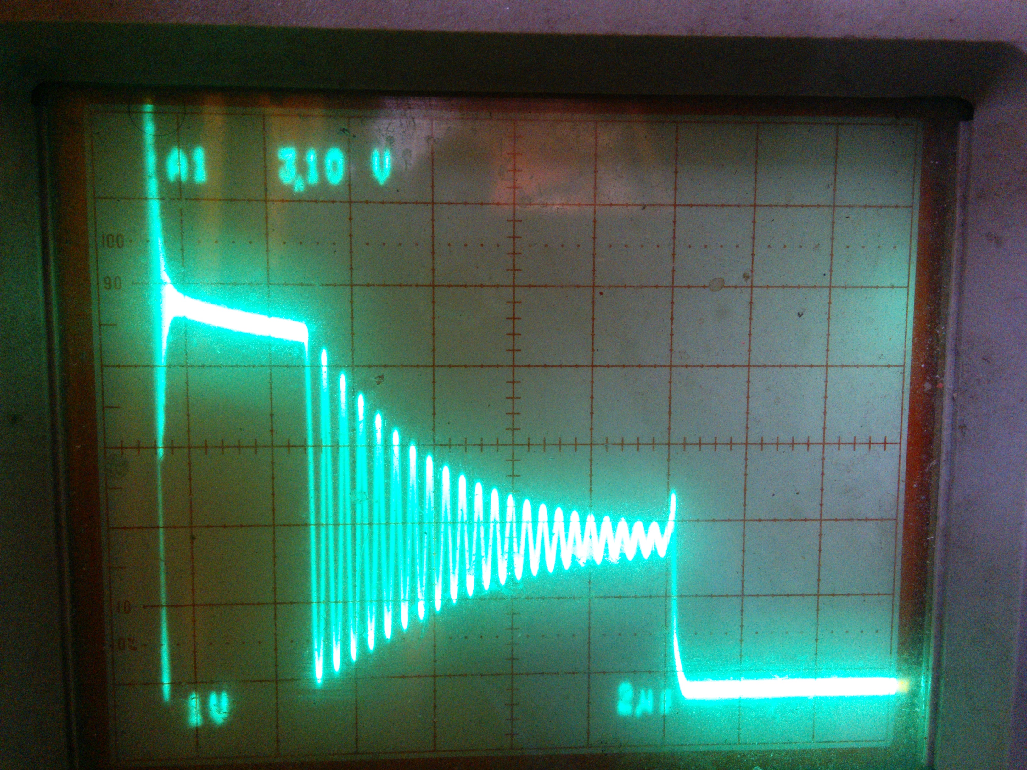
I have designed a circuit in which the input can be anywhere in the range of 11 to 26 volts, and the output is adjustable from 2 to 40 volts at up to 5 amps.  It's working OK, but the boost Mosfet is getting hotter than I think it should when the circuit is boosting the input voltage.  If the output voltage is less than the input voltage I still see the ringing, but heating is not a problem because at lower output voltages the load current is much less. . Looking at the waveform on a scope, there is a lot of ringing on the inductor. I'm not seeing much of the ringing on the gate of either Mosfet. I've tried changing the oscillator frequency and changing the inductor, and I can change the appearance of the ringing, but it's always there.  If this is normal I'll just add more heat sink to the boost Mosfet.  What do you think?

On the attached waveform the vertical scale is actually 10 volts/div (10X probe).  

  • Heating the MOSFET is not caused by the ringing that you show on the scope, but by the much high frequency ringing at the rising edge of the waveform which is seen shoot up to the celling of the scope screem. It increases the switching losses at turnoff transient. The ringing tail of the waveform does not cause much losses because the switch is already off and the ringing is just the resonance beween the switch Coss and the inductor.

    The ringing tail is the natural behavior in a switch mode power supply when it runs in discontinuous conduction mode (DCM). Please check a power electronics text book to learn the difference between the DCM and the continuous conduction mode (CCM). If you see the ring tail at full power, that means your inductor is not big enough. You should select an inductor such that you only get into DCM at <20~40% rated load. Please use our online tool Webench to help you to get a proper design.
  • Thank you very much for your reply. That information is VERY helpful.  I mainly design with analog and logic circuits, so this is a bit out of my comfort zone.

    I changed to a different inductor, changed the oscillator frequency, and modified the gate drive circuit. Does this look better to you?

    BTW- I did start out by using Webench, but since I needed to vary the output voltage over a wide range I'n not sure I did it correctly.

  • Hi Rick,

    The waveform does look like it has less ringing on the rising edge of the waveform which is better. As Youhao mentioned reducing this peak voltage will help to reduce the switching losses. A snubber can be added to reduce this peak voltage if the MOSFET is still getting hot. Also optimizing layout will help to reduce parasitics which in turn will reduce ringing.

    Thanks,

    Garrett
  • Thanks, Garrett!!