Hi all
Would you mind if we ask TPS3702?
<Question1>
The datasheet shows the typical value of tpd(HL) and tpd(LH).
Do you have the mininum value and maximum value of them?
We guess that you do not test this spec in production for every device, you do not guarantee a minimum and maximum value.
<Question2>
The datasheet shows the typical value of Tsd(Startup delay).
Do you have the mininum value and maximum value of this?
We also guess that you do not test this spec in production for every device, you do not guarantee a minimum and maximum value.
<Question3>
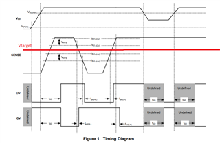
There is the description "During the power-on sequence, VDD must be at or above 2 V for at least tSD before the output is in the correct state." on the datasheet.
After VDD is above 2V, during Tsd(typ 300us), what will the status of the output pins OV and UV are?
It seems that UV is low and OV is high.
And does "Undifined" mean Hiz?
Is our recognition correct?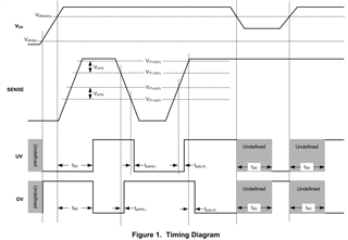
<Question4>
Does the any power sequence between VDD and SENSE?
We quess that there is no the any power sequence between VDD and SENSE.
As the background of this question, our customer would like to insert these voltage the same time.
Kind regards,
Hirotaka Matsumoto

-
Ask a related question
What is a related question?A related question is a question created from another question. When the related question is created, it will be automatically linked to the original question.