This thread has been locked.

If you have a related question, please click the "Ask a related question" button in the top right corner. The newly created question will be automatically linked to this question.

ISO5451: DESAT protection mechanism

Part Number: ISO5451

I did some test yesterday. I have some questions about ISO5451's DESAT protection mechanism.

Phenomenon:

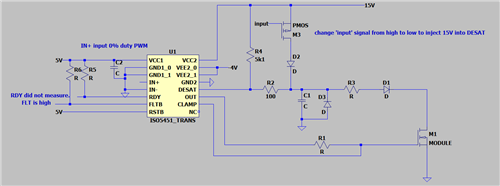
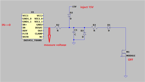
I forced IN+ to low, then injected 15V into the DESAT pin through an external supply via a resistor and a diode, after that measured the voltage of DESAT pin and FLT pin refer to the diagram below. I noticed that the DESAT pin is vibrating and the FLT pin is high refer to the waveform below.

Diagram:

Waveform:

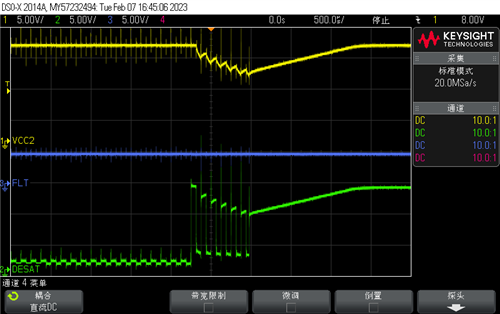
Yellow line is VCC2; Blue line is FLT; Green line is DESAT.

Questions:

1.Is that mean during the power module shutdown or say the IN+/OUT is low, the DESAT function is inactive?

2.The DESAT pin has an internal mos, according to my understanding, during the power module is off, the DESAT pin is kept low internally by turn on the internal mos, the internal current source is switched off, is that right?

3.Could you explain why the waveform of DESAT pin is like that? Because of the turn on and turn off of the internal mos?

  • Hi Pengfei,

    "Is that mean during the power module shutdown or say the IN+/OUT is low, the DESAT function is inactive?" - thats right.

    2.The DESAT pin has an internal mos, according to my understanding, during the power module is off, the DESAT pin is kept low internally by turn on the internal mos, the internal current source is switched off, is that right? - thats right.

    3.Could you explain why the waveform of DESAT pin is like that? Because of the turn on and turn off of the internal mos?

    The internal mos is always pulling DESAT pin to COM when INP is LOW.  Let me get back to you on the pulse behavior. 

    Thanks

    Sasi

  • Hi Pengfei,

    "Is that mean during the power module shutdown or say the IN+/OUT is low, the DESAT function is inactive?" - thats right.

    2.The DESAT pin has an internal mos, according to my understanding, during the power module is off, the DESAT pin is kept low internally by turn on the internal mos, the internal current source is switched off, is that right? - thats right.

    3.Could you explain why the waveform of DESAT pin is like that? Because of the turn on and turn off of the internal mos?

    The internal mos is always pulling DESAT pin to COM when INP is LOW.  

    1. Are the 15V supply to the DESAT pin tied to the VCC2?  I see VCC2 getting pulled low as well. 

    2. What is the current  limit of the supply? Its possible the test may inject more current into DESAT pin which will break the device if it exceeds 14mA for longer duration due to increased temperature.

    What is the purpose of this exercise?

    Thanks

    Sasi

  • Thank you so much for the reply. Now I clearly understand the mechanism of DESAT when the INP is low.

    Next question is,

    3.Could you explain why the waveform of DESAT pin is like that? Because of the turn on and turn off of the internal mos?

    The internal mos is always pulling DESAT pin to COM when INP is LOW.  

    1. Are the 15V supply to the DESAT pin tied to the VCC2?  I see VCC2 getting pulled low as well. - Yes, the supply I injected to DESAT is VCC2.

    2. What is the current  limit of the supply? Its possible the test may inject more current into DESAT pin which will break the device if it exceeds 14mA for longer duration due to increased temperature. - The capability of the supply does not exceed 100mA. So the current may exceed the limit of the internal circuit. Whether the oscillation of DESAT was caused by the internal mos's turn on and off in order to protect the component and internal circuit?

    What is the purpose of this exercise? - Because I want to know how the DESAT pin's internal circuit works when the INP is low (because the datasheet does not refer to), so I did this test and asked this question to validate my understanding and want to get TI's acknowledgment.

  • Thanks Pengfei for your inputs. Based on the schematics shared, we couldnt understand the DESAT pin voltage behavior. Unless you share the full system schematic and additional pin conditions and voltages. It may not be easy to explain it.

    What initated the pulses? Is the device still functionnig?

  • Thank you for your reply, Sasikala. 

    The addition pin conditions and voltage refer to the diagram below. How I injected 15V is also mentioned.

    The RDY pin did not be measured, it should turn to low according to the VCC2's falling down.

    The IN+ input 8kHz 0% duty PWM may cause the pulse. Yes, the device is still functioning.

    Please help me analyze.

    Thanks!

  • Hi Pengfei,

    If you have triggered IN+ high then ofcourse, that explains why the DESAT pin will oscillate based on if the DESAT is triggered for the threshold condition or not. 

    But I dont undertand about = IN+ 8Khz- 0% duty cycle - what that means? 

    Please refer the following technical guide which explains about the DESAT functionality.

    https://e2e.ti.com/support/power-management-group/power-management/f/power-management-forum/1096147/faq-gate-driver-faq-frequently-asked-questions

    I believe that the link explains the details what you are looking for. If it solves your questions, please press "resolved" button.

    Thanks

    Sasi

  • Hi Sasi,

    I am sorry for not explaining clearly the meaning of 8Khz- 0% duty cycle. We have a test device which can inject PWM to IN+, so the 8kHz-0% means forcing IN+ to low.

    Thank you for your help.