This thread has been locked.

If you have a related question, please click the "Ask a related question" button in the top right corner. The newly created question will be automatically linked to this question.

LM51561H-Q1: application inquiry

Part Number: LM51561H-Q1
Other Parts Discussed in Thread: LM5156

Hello boost Team,

I have 3 questions below.

1) Datasheet, 9.3.13 MOSFET Driver (GATE Pin)
In the datasheet, there is instruction Qg @ VCC * fsw < 35mA.
I suppose this is the case of connecting Cvcc to GND like below.


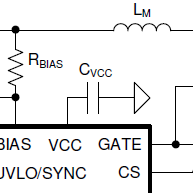
This fomula is not applicable, if Vcc supplied from external power source, correct?


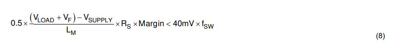
2) Application note SNVA941A for LM5156 boost

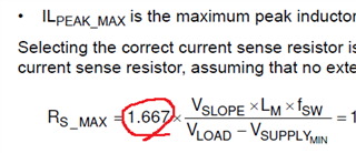
There is description of setting Rs_max, where does the figure 1.667 come from?

3) Generally PDS design & reference board place gate resistor.
If you have advice how to choose gate resistance, please let us share.

Regards,
ti

  • Hi Tosh,

    Thank you for using E2E forums, regarding your query:

    1. if the VCC is externally supplied and the provided voltage is sufficient to turn the MOSFET on then yes this formula is to be avoided as this formula is for internal VCC regulator meaning when we are using the internal VCC instead of external.

    2.  This formula is for the maximum Rcs based on the internal slope compensation, and the 1.667 value comes from the ratio of the slope compensation to down slope which can be altered to give more margin.

    3. For the gate resistor here is an interesting tech note https://www.ti.com/lit/an/slla385a/slla385a.pdf?ts=1676034729967&ref_url=https%253A%252F%252Fwww.google.com%252F 

    Hope this answers your questions.

    BR,

    Haroon

  • Hello Haroon,

    Let me ask you more about answer #2.

    In your comment "the 1.667 value comes from the ratio of the slope compensation", could you tell the exact calculation to figure out 1.667?
    The slope is 30uA, I don't reach to be 1.667.

    The application note SNVA941A is instruction for boost.
    Please share info if you have SEPIC mode.

    ti

  • Hello Tosh,

    Equation (6) in the Application Note is derived from Equation (8) in the datasheet, using 20% of margin and ignoring the Diode forward voltage VF.

    1 / (0.5 * 1.2)  =  1.667

    Best regards,

    Harry