This thread has been locked.

If you have a related question, please click the "Ask a related question" button in the top right corner. The newly created question will be automatically linked to this question.

TPS62746: TPS62746

Part Number: TPS62746

Short Summary:
We are finding a high % of boards we build get bad after a few cycles of battery charging.
The part that gets damaged is the 1.8V bouck regulator: TPS62746YFPR

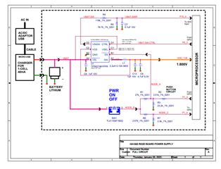
Please find attached the section of the schematics that includes the power supply and the push-button ON/OFF control.

Short description of the circuit:
A single-cell rechargeable lithium battery is connected to VIN pin U1, TPS62746YFPR, which is a buck regulator that outputs 1.8V.
The 1.8V powers the microprocessor. All ports of the uP are powered from this 1.8V.
To start the circuit, push-button SW1 is pressed and through the R1/R3 divider the EN pin receives a signal to turn ON the buck.
Once the uP receives power and boots, it will drive P1_3 high (close to 1.8V) and through R2 will keep the EN pin HIGH, and the buck in ON state.
To stop the circuit: If uP is running, a long press on the SW1 will be detected as a logic HI on P1_4 (which works as an input) and under SW control, P1_3 will be driven low. This will cause the EN pin to go low and stop the circuit.

Damaged Boards
We found a high number of boards presenting an increased leakage on VBAT. We measure a resistance of a few hundreds of Ohms.
While the boards may still work (buck still outputs regulated 1.8V), when the circuit is turned off, there is still significant current consumption from the battery, which causes the battery to be over-discharged.

Damaged Device Measurements
We removed 3 devices from boards.
I measured one of the devices:
- VIN-VSEL = 7.3... 8 Ohm, both directions (short)
- VIN-GND = 480... 481 Ohm both directions (partial short)
- VSEL-GND = 475... 476 Ohm both directions (partial short)
- VIN-VINSW = 3.6... 3.9MOhm both directions (normal)
- EN - GND = internal ESD diode 0.7V, normal

Based on the above, the part has two things damaged:
- VSEL is shorted partially to GND
- VSEL is shorted strongly to VIN
I don't think VIN is shorted to GND because the part continues to work, but with the extra leakage.
So, somehow the VSEL pin gets damaged.
My best guess about the cause:
The EN and VSEL pins are not Schmitt Trigger inputs (no hysteresis) and somehow the logic gets into an illegal state that creates a shoot-through current on the VSEL I/O cell.
This can happen when the circuit is left ON, and the battery is discharging slowly, and may reach some voltage levels that cause this scenario.
It could be also possible that the switch generates a bouncy signal, and the buck's internal logic gets confused because it is not Schmitt trigger type, enabling some unintended path that creates an internal short circuit.

The datasheet does not explicitly allow or disallow connecting VSEL directly to VIN, while EN pin is controlled separately. Can you clarify if there are any restrictions? Or VSEL must nut be high before EN? Should we tie VSEL to EN instead of VIN?
Can the circuit go into an illegal state if EN is between LOW and HIGH (0.4V to 1.1V)?

We would greatly appreciate TI's support on this urgent issue that causes us to stop production. We have a line down situation.

  • Hello Nilesh,

    Thank you for reaching out. 

    What is the Vin to the device? and can you please check the input current of the device with the following conditions to check weather the leakage is due the device itself or due some other source.

    The datasheet does not explicitly allow or disallow connecting VSEL directly to VIN, while EN pin is controlled separately. Can you clarify if there are any restrictions?

    There should not be any concern connecting VSEL and EN pin directly to VIN.

    I will get back to you with more inputs based upon your measurement results.

    Thank you,

    Regards,

    Moheddin.

  • ============================
    Q: What is the Vin to the device?
    A: The VIN to the device is one Li-Ion rechargeable cell, so the voltage maximum is 4.25V.
    Q: And can you please check the input current of the device with the following conditions to check whether the leakage is due the device itself or due some other source.
    A: Every other component connected to VIN on the board was removed, the input current to the board was high with the only device left the TI buck TPS62746YFPR.
    We removed the buck from the board and measured the device directly on its pins. It shows a resistance in the range of a few hundreds of Ohms between VIN and GND.
    We also found VIN shorted to VSEL. Repeated the steps for 3 failed boards.
    We measured one of the devices:
      - VIN-VSEL = 7.3... 8 Ohm, both directions  (short)
      - VIN-GND = 480... 481 Ohm both directions (partial short)
      - VSEL-GND = 475... 476 Ohm both directions (partial short)
      - VIN-VINSW = 3.6... 3.9 MOhm both directions (normal)
      - EN - GND = internal ESD diode 0.7V, normal
    Based on the above, the part has two things damaged:
    - VSEL is shorted partially to GND
    - VSEL is shorted strongly to VIN
    I don't think VIN is shorted to GND because the part continues to work, but with the extra leakage.
    So, somehow the VSEL pin gets damaged.
    My best guess about the cause:
    The EN and VSEL pins are not Schmitt Trigger inputs (no hysteresis) and somehow the logic gets into an illegal state that creates a shoot-through current on the VSEL I/O cell.
    This can happen when the circuit is left ON, and the battery is discharging slowly, and may reach some voltage levels that cause this scenario.
    It could be also possible that the switch generates a bouncy signal, and the buck's internal logic gets confused because it is not Schmitt trigger type, enabling some unintended path that creates an internal short circuit.
    We have a serious issue that causes a line down situation.  Please escalate, this is urgent for our company.  We have hundreds of finished products that we cannot ship.
    Thank you.
  • Hello Nilesh, 

    1.Connecting VSEL directly to VIN, while EN pin is controlled separately?

    There should not be any problem.

    2.Is there any problem if the VSEL is pulled high before EN?

    As per the datasheet, the voltages of VSEL and EN are related to VIN, there should not be a problem.

    3.Does the circuit go into an illegal state if EN is between LOW and HIGH (0.4V to 1.1V)?

    No, as per the absolute max of the datasheet.

    Regarding the schematic:  I would recommend to use minimum 4.7 uF for input capacitor.

    We also found VIN shorted to VSEL. Repeated the steps for 3 failed boards.
    We measured one of the devices:
      - VIN-VSEL = 7.3... 8 Ohm, both directions  (short)
      - VIN-GND = 480... 481 Ohm both directions (partial short)
      - VSEL-GND = 475... 476 Ohm both directions (partial short)
      - VIN-VINSW = 3.6... 3.9 MOhm both directions (normal)
      - EN - GND = internal ESD diode 0.7V, normal

    How you measured the resistance between the pins of the device? you mentioned that you removed the device from the board and then measured the resistance, but there is also a possibility that it might have damaged during the desoldering. This data defines that the device is damaged.

    What i would recommend is to check the input current that device is drawing without load and compare that with the quiescent current in the datasheet. 

    can you please check the input current of the device with the following conditions to check weather the leakage is due the device itself or due some other source.

    While the boards may still work (buck still outputs regulated 1.8V), when the circuit is turned off, there is still significant current consumption from the battery, which causes the battery to be over-discharged.

    Please provide me the VIn, Vout and SW waveforms of the existing device on your board. Can you also provide me the layout.

    In order to further debug the issue i need the above requested data. 

    Thank you,

    Regards,

    Moheddin.