This thread has been locked.

If you have a related question, please click the "Ask a related question" button in the top right corner. The newly created question will be automatically linked to this question.

LP87524B-Q1: How to achieve such a low 4MHz tone in data sheet Fig.79 (<2uV)?

Part Number: LP87524B-Q1

Hi there,

We are reading the data sheet and trying to get good performance out of this part. Below is the data sheet I refer.

https://www.ti.com/lit/ds/symlink/lp87524j-q1.pdf?ts=1676360173340

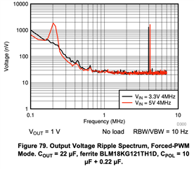
In Fig. 79. I pasted below. The 4MHz tone is <2uV. This is so much below the 4mV output voltage ripple, shown in spec table in Page 7 of the same data sheet. Could you please let me know how to achieve this performance?

  • Hi Hank,

    Please see the Layout section of the datasheet for full recommendations. The most important recommendations for this are #1 and #2:

    "1. Place CIN as close as possible to the VIN_Bx pin and the PGND_Bxx pin. Route the VIN trace wide and thick to avoid IR drops. The trace between the positive node of the input capacitor and the VIN_Bx pin(s) of LP87524B/J/P-Q1, as well as the trace between the negative node of the input capacitor and power PGND_Bxx pin(s), must be kept as short as possible. The input capacitance provides a low-impedance voltage source for the switching converter. The inductance of the connection is the most important parameter of a local decoupling capacitor — parasitic inductance on these traces must be kept as small as possible for proper device operation. The parasitic inductance can be reduced by using a ground plane as close as possible to top layer by using thin dielectric layer between top layer and ground plane.

    2. The output filter, consisting of COUT and L, converts the switching signal at SW_Bx to the noiseless output voltage. It must be placed as close as possible to the device keeping the switch node small, for best EMI behavior. Route the traces between the LP87524B/J/P-Q1 output capacitors and the load direct and wide to avoid losses due to the IR drop."

    Thanks,

    Daniel W

  • Hi Daniel,

    Maybe you misunderstood what I said. 

    What I said is, the datasheet of this part shows 4mV voltage ripple spec. However, in Fig 79 as I showed in my post, the ripple is below 2uV. Is the testing data not correct? Please take a close look at Fig 79. Zoom in to see the height of the tone at 4MHz.

    Thanks

    Hank

  • Hi Hank,

    The 4mV is a typical spec for the total output ripple. The above figure is a specific example application curve with the spectral break down of the output ripple.