


Hello TI Support Team,
we are using the UCC21732 gate drivers for a high power inverter (1000VDC, 500Arms) and have problems with dubious error signals RDY and /FLT.
A. In case of the RDY (UVLO) signal we already see at 500VDC and higher currents (>600Apk) a metastable "Low" Signal for some µs instead of tRDYHLD=0,55...1ms.
Please see schematic (*.zip) and measurements: 20230222_3:44:11PM, _3:41:23PM:
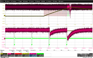
C2/Z2 (rd) D5/12-D5/9: RDY-signal directly measured at pins
Z4: VDS of Top-Switch
(Note to C2/Z2: The noisy signal is due to the optical probe HVFO103 at high resolution)
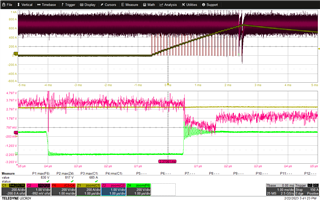
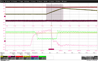
We checked the VCC-voltage --> _3:49:48PM
Z2 (rd) D5/15 (VCC) - D5/9 (GND)
Z3 (bl) (=Z2 with LowPassFilter 5MHz)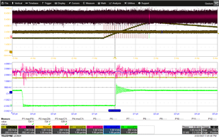
We checked the VDD-voltage --> _3:58:20PM
Z2 (rd) D5/5 (VDD) - D5/3 (COM)
Z3 (bl) (=Z2 with LowPassFilter 5MHz)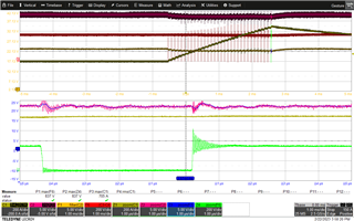
In both cases there is no undervoltage visible.
B. Concerning the /FLT signal we only can operate the inverter above 500Apk with shorted OC-input:
Without shorting OC there is a /FLT (desat) signal although there is definitively no 2-Level-Turn OFF. --> 20230221_11:26:55PM
C2/Z2 (rd) VGS_Top-Switch
Z4 (gn) VDS_Top-Switch.
Shortly after turn ON the UCC gate driver switches OFF with failure signal /FLT, but not with 2-Level-TurnOFF V2LOFF=9V.
Do you have an idea what's wrong?
Regards, Karl

