This thread has been locked.

If you have a related question, please click the "Ask a related question" button in the top right corner. The newly created question will be automatically linked to this question.

LM62460: re-work debug on customer's board.

Part Number: LM62460
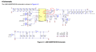
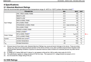
Other Parts Discussed in Thread: LM61495RPHEVM, ,

Hi team,

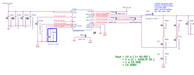
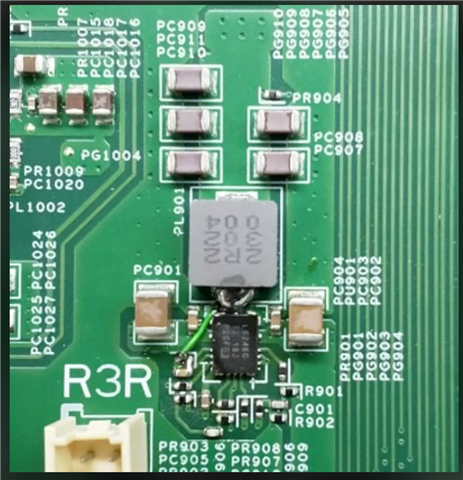
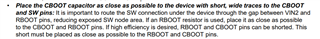
my customer mistaken the Cboot connection as you can see in the schematic here.

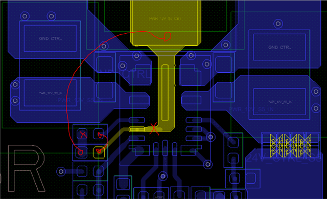
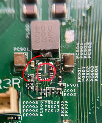
they tried to re-work on the board with single-core wire ,

1. they first cut off the connection between the SW and  Cboot

2. they use a wire to connect Rboot pin and Cboot pin

3. last, they use another long, thin one core wire to connect Cboot cap to SW.

but the Vin pin damaged right after they test full-load transient,  is there anything we miss during the re-work?

is the long, thin one core wire for connection acceptable here?

  • Hello,

    Below is the LM61495RPHEVM schematic. Highlighted in red is the CBOOT,RBOOT,SW connection that should be implemented on your board.

    The connection between CBOOT and SW should be as small as possible so as to create a small SW node. Having a long wire loop that connects CBOOT to SW would add unneeded inductance that can couple noise to SW which is undesirable. 

    The easiest way would be to cut the trace that directly connects CBOOT to SW and solder a wire that connects CBOOT capacitor to CBOOT pin.

    Regards,

    Jimmy

  • Hi Jimmy,

    this issue is quite series since they don't have much board at this stage, our part may be removed if we can't re-work succesfully, can you guide us ?


    1. I think your suggestion was only base on our schematic,  please help check layout again.

    one way or another, we have to solder a trace to connect Cboot to SW, but the thing is how long and how thick should this wire be.

    2.and  was this long, thin wire the root cause of this transient damaged?  unneeded parasitic inductance could cause this?

    if yes, please explain it to me, they are trying to know the root cause since they only have "one" board left can be tested now.

  • Hi,

    Is the customer just evaluating their prototype system board? I would not recommend this rework in actual application but just to solve the customer's issue. 

    1. Yes this rework would put CBOOT capacitor between CBOOT (Pin4) and SW (Pin16). The trace should be as small and thin as possible to minimize noise coupling.

    2.  When they wire the SW, they need to be extra careful to not accidently short the SW to GND or VIN. If it was not a proper solder job and the wire accidentally touched either GND or VIN on the input capacitor exposed terminals, then this will cause damage to the internal FET. Refer to the Pin FMA for SW short circuited to GND and SW short circuited to supply (https://www.ti.com/lit/fs/snva981a/snva981a.pdf). 


    3. Please describe in more details what the test that was done that caused VIN to be damaged. What is the VIN and IOUT transient? Was the device operational, switching at 400kHz and regulating to 12V output without the IOUT transient? 

    Regards,

    Jimmy

  • HI Jimmy,

    they need to re-work to check the IC is ok, even though they did wrong at the schematic.

    please see the re-work picture.

    1. I thought the boot connection should be wider instead of thinner?

    2.3. about question 2 and 3,

    yes, they were doing fine and ok when steady state loading(<3.3A) , but only damaged at 30%~100% load transient(1.8~6A), which shows that it's not just shorting problem. 

    BTW, Vin=24V, Vout=12V, 400KHz, and the transient damaged was happened 10s after  the transient started.

    so is this wire parasitic may potential cause this damage?

  • Hi,

    1. You are correct, it should be short and wide, not thin. The short and wide SW node will have lower inductance. 

    2. That is good to know that the device is regulating at steady load. It would be good to have a SW, IOUT and VOUT waveform at steady state just to confirm proper switching. The customer will obviously need to relay out their board to follow the recommended guidance for the component placement and connection but at least this provides that the design is regulating and operating.

    3. The extra wire introduce unwanted parasitic on the SW node and during a load transient, it is possible that it is overstressing the abs max spec of the SW see below. The extra wire loop connection may result in a larger SW node ringing than typically expected especially when the part is excited with a load transient. 

    If the customer is still not convinced, I would suggest taking the LM62460RPHEVM with proper layout, configure it for 12V output, output inductor and switching frequency and demonstrate to customer that device is operating for their transient condition.  

    Regards,

    Jimmy 

  • Hi Jimmy,

    one thing I don't understand is that,

    the wire is between Cboot and SW ,but SW pin level is usually either Vin-Vout or 0  depends on the phase,

    so I don't get it why this wire will affect the SW voltage ringing. and why it affect a lot especially in transient.

    would you elaborate it more in detail?

  • Hi,

    Just to be clear, the LM62460 is a buck converter that is capable of being used in an application like the customer's use case of 24Vin|12.2Vout|400kHz|IOUT up to 6A and should not have any issues doing so as long as PCB layout and schematic connection is followed per datasheet spec. The application customer has for this device is normal, and can even be designed with Webench

    Below is what is stated in the datasheet, highlighting the importance of reducing the SW node area as much as possible. The rework with the extra wire on CBOOT back to SW increases the SW node area which will impact SW voltage ringing. This does not mean that the wire is the main cause of the blow up, but it can be a contributing factor that is non-ideal in a typical PCB layout design. 

    Also I would suggest having a bulk electrolytic input bulk capacitor with moderate ESR (~100-200mOhm) to dampen the input. Usually when input VIN is damaged, it is caused from EOS during testing. 

    For the damaged part when customer did the load transient, did they remove the unit and check continuity on the device itself? Is VIN shorted to GND, etc.? 

    What would be important and have customer provide waveform of is the following:

    • First I would suggest customer isolate just this circuit and directly power the input with a stable power supply with appropriate input current limit (3-3.5A). 
    • Provide Vout and SW waveform for steady state with loading at both typical application and max loading (3A and 6A). Since this device is a LM62460, it should be able to load current up to 6A. This exercises standard operation of the device. 
    • Use a controlled electronic load set to CC mode and perform load transient test (50% to 100%). Provide waveform of this. 

    Regards,

    Jimmy

  • HI Jimmy,

    if rework wire will bring extra area, then we should use thin wire instead of thick wire, right?

    we were back and forth on this, so just want to confirm on this change.

    and like I said , they don't have much shot, so we can arrange this test after confirming change list to prevent damage again

  • Hi Fred,

    The trace should be as short as possible. I doubt there will be significant difference between thin and thick gauge wires so long as customer is not making a long SW loop. 

    Does customer have feedback on my previous questions "For the damaged part when customer did the load transient, did they remove the unit and check continuity on the device itself? Is VIN shorted to GND, etc.? ". I'm assuming they will replace the damaged unit and test with a new unit. Please have customer also test on a different new reworked board just to get more sample points.

    I am expecting to hear back from customer on the test:

    • New unit on old reworked failing board
    • New unit on new reworked board 

    Regards,

    Jimmy

  • Hi Jimmy,

    there's no way to test continuity,

    1.the board has damaged as well, a hole has been burned out.

    2. Vin pin is confirmed shorted to GND.

    please provide further guildline for us  thanks

  • Hi Fred,

    As stated previously, on a brand new undamaged board:

    • Isolate the circuit by supplying an input voltage from a stable power supply with appropriate current limiting. For the load current, suggest using an electronic load on the output. Suggest limiting the input current to around 3-3.5A. This should prevent any potential damage to the part during testing. 
    • SW trace should be as small as possible to minimize inductance on SW. Be careful not to accidentally short SW to VIN or GND as this is a Class A failure effect that will permanently damage the part and will cause VIN to short to GND internal to device. Pin FMA (https://www.ti.com/lit/fs/snva981a/snva981a.pdf). 
    • If there is an input EMI filter or  long input lead traces, then it is recommended to have a bulk electrolytic capacitor with moderate ESR (~100mOhm - 200mOhm) to help dampen the input. 

    Regards,

    Jimmy 

  • HI Jimmy ,

    May I know why add bilk electrolytic cap instead of MLCC at input?

    I though MLCC has lower ESR and better response?

  • Hello Fred,

    The electrolytic bulk capacitor is used in addition to the recommended input MLCC capacitor. As mentioned previously the bulk cap is used to dampen the input if there is an input EMI filter or long input leads from supply to input pin. Refer to app note for more details on this. 

    app note:https://www.ti.com/lit/an/snva489c/snva489c.pdf#page=6

    Regards,

    Jimmy