This thread has been locked.

If you have a related question, please click the "Ask a related question" button in the top right corner. The newly created question will be automatically linked to this question.

TPS650864: PMIC is in Power fault state during board bring-up with ZU3 FPGA

Part Number: TPS650864
Other Parts Discussed in Thread: BOOSTXL-TPS650861

Hello James Steenbock

Hope you remember me and the issues that we had discussed in above chat previously very long ago.

In the last message, I had mentioned that we shall build a new PCB with TI suggested changes and test it and provide feedback. 

Finally, we build the PCB with TI suggested changes and tested it. But unfortunately, when we turned ON the board, PMIC was still in Power fault state. As usual we continued to debug the issue which caused the power fault in this PMIC. Below are our observations in CASE1 and CASE2,

CASE1: 

1)  We verified input & output rails and found to be correct VSYS=12V, LDO3P3=3V3, LDO5P0 =5V0, Vref=1V2 and V5ANA=5V0. 

2) Then we started to debug the BucK1-6, VTT and LDOA1-A3 and found that PMIC was in power fault state. 

3) We also wanted to check if the IC from reel had any fault, to test this we used TI BOOSTXL-TPS650861 Evaluation board | TI.com. With this we can provide CTL1 to 6 inputs to start the PMIC sequence and check the respective rails for pre-programmed PMIC IC TPS65086401RSKT. as per our design we need to provide only 3 inputs to CTL pins (CTL1, CTL6 and CTL4 in same order or sequence)

4) when we provided CTL1 and found that associated power rails were up without any power Fault and GPO1 was ON

5) when we provided CTL6 and found that associated power rails were up without any power Fault and GPO2 & GPO3 was ON (But as per sequence only GPO3 was supposed to be ON)

6) when we provided CTL4 and found that PMIC entered into power fault state and so we just removed CTL4 to see if PMIC recovered from power fault and yes it did.

Summary: A brand new PMIC IC TPS65086401RSKT from the reel when tested with Eval board was showing power fault. To confirm this behavior, we removed the input CTL4 on our newly build board and found that PMIC was able to recover from power fault although the rails associated with the CTL4 were not up. 

CASE 2:

From the case history we had concluded that, if the required caps were not provided for unused pins like (LDOA1, LDOA2, LDOA3, SWA1, SWB1 &SWB2) then we can use a custom OTP programmed PMIC with Part # TPS65086100 and disable these pins. We did try this and following were the observations,

1) We programmed our custom OTP into Blank PMIC IC TPS65086100 and replaced it with our pre-programmed IC on our newly build boards to mitigate the above CASE1 issue.

2) After replacing the IC with OTP IC and did a power ON, initially it seems all the rails were working, but when we did a power cycle, we saw PMIC went to power fault state. 

Buck1: 1V8 without power fault

Buck1: 1V8 with power fault

3) after providing a time gap of about 10mins and then when we turned ON the board the PMIC was seen functioning normal without any power fault. But didn't stay for long and just entered again into power fault state.

Summary: the issue that we are facing here is, every time we do a power cycle to OTP burned PMIC we need to provide a delay of around 10mins or so. and sometimes it may be more. Hence case2 is also not helping us to resolve issues faced in case1. We are seeing some inconsistence with respect to PMIC's behavior.

Since this build of boards were for customer delivery, we are not able to delivery any hardware till now and struggling to resolve this PMIC related issue. Hence, I would request you to please support us in resolving this issue as its turn out to be a critical issue and blocking our delivery to customer.

The schematics of PMIC is already with you.

Old case details: TPS650864: Troubleshooting PMIC behavior used to power Xilinx ZU3. - Power management forum - Power management - TI E2E support forums

Let me know if you have any other questions. 

Best regards,

Sandeep P

  • Hi Sandeep,

    5) when we provided CTL6 and found that associated power rails were up without any power Fault and GPO2 & GPO3 was ON (But as per sequence only GPO3 was supposed to be ON)

    1) The TPS65086401 should have a pre-programmed power up sequence. I double checked our OTP configuration document and according to the sequencing section, pulling CTL1 "high" should cause GPO1 and GPO3 to be enabled (assuming all associated rails reach PGOOD status). Can you clarify why GPO3 is expected to turn on only after CTL6 is pulled "high"? Based on the sequence CTL1 should lead to GPO1 and GPO3 being enabled and CTL4 should lead to GPO2 being enabled.

    You mentioned that your ICs were brand new from the reel so I would not expect them to have a different programming. Right now the expectations you mentioned don't line up with the default OTP settings for the TPS65086401.

    Below is a picture of the sequence settings that are in the TPS65086401 OTP document:

    If removing CTL4 causes the PMIC to recover from fault status, then this is the first place we should check for issues but at the moment I am unsure about the expected device behavior.

    2) I'll take a look at your schematic. Can you share your custom OTP excel document with me so I can review the settings?

    Regards,

    James

  • Hi James,

    1) The TPS65086401 should have a pre-programmed power up sequence. I double checked our OTP configuration document and according to the sequencing section, pulling CTL1 "high" should cause GPO1 and GPO3 to be enabled (assuming all associated rails reach PGOOD status). Can you clarify why GPO3 is expected to turn on only after CTL6 is pulled "high"? Based on the sequence CTL1 should lead to GPO1 and GPO3 being enabled and CTL4 should lead to GPO2 being enabled.

    My bad, you are correct, as per sequence GPO1 and GPO3 goes high once CTL1 is "high" (I mixed up the custom sequence with Pre-programmed sequence while explaining to you). But the point that we observed with band new IC (TPS65086401RSKT) is after we provided CTL4 as high the PMIC would go into power fault state. I am really not sure what is the cause for this as we are testing it with BOOSTXL board, and it matches with the behavior on our brand-new board which we powered up only once and it was seen in power fault state. The other observation is GPO2 never turns ON.

    2) Please find the custom OTP excel for your review. We have optimized the sequence to start with CTL1 followed by CTL6 and last CTL4. based on attached power sequence PDF. 

    BASE_PMIC_TPS65086100 OTP Generator V2p5.xlsx Power_Sequencing_ArchitectureV1.1.pdf

    Best regards,

    Sandeep P

  • Hi Sandeep,

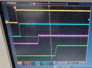
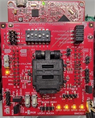
    1) I checked your custom OTP on a BOOSTXL board and found that BUCK3, LDOA3, and BUCK5 were able to ramp up to the target voltage without causing a power fault. Below is a scope capture of the CTL4 event and also a picture of my BOOSTXL board so you can see which jumpers I have connected.

    Scope Capture of CTL4 sequence - CH1: CTL4, CH2: BUCK3, CH3: LDOA3, CH4: BUCK5

    Picture of BOOSTXL-TPS650861 Evaluation Board

    Here you can see that GPO2 has been successfully pulled "high" to indicate good rail regulation.

    This was done without any loading of the output power rails to make sure there were no issues with the sequence programming itself.

    2) I also tested a chip programmed with the TPS65086401 OTP settings in the BOOSTXL board to see if there were any issues with the CTL4 sequence. It is important to check the jumpers at J14 on the BOOSTXL board. These jumper can be seen in the top right of the BOOSTXL board picture above. These jumpers handle the input supplies to SWB1 / B2, SWA1, and LDOA2 / A3.

    For the TPS65086401, SWB1 and SWB2 are set to 1.8V. If you supply the PVINSWB1_2 pin with 3.3V using the 3V3_EVM source pin (just below PVINSWB1_2) the IC will encounter a power fault since SWB1 and SWB2 are looking for 1.8V PGOOD.

    In order to properly test the TPS65086401 using the BOOSTXL board, I would suggest connecting the BUCK1 1.8V output to PVINSWB1_B2 so that the two load switches have the correct voltage for PGOOD checks. LDOA2, LDOA3, and SWA1 can still be powered using the 3V3_EVM source pin.

    From your schematic, it looks like you are currently supplying the Load Switches with LDO5P0. This would cause a power fault on the TPS65086401 since this voltage is too high for the PGOOD target.

    You will likely need to supply the Load Switches with one of your bucks (BUCK1 for example) or with an external input source.

    You may notice that in your custom OTP you have all the load switches disabled, so the jumper configuration should not cause a power fault with the custom programmed IC.

    Let me know if you have other concerns.

    Regards,

    James

  • Hello James,

    Thanks for your detailed reply. 

    The findings regarding the PVINSWB1_B2 pin input voltage was correct. Although while debugging i had found out that 5p0 was given as incorrect input voltage and did a rework on board to remove the rails PVINSWA1 and PVINSWB1_B2 from 5p0 and connected it to 3p3. But unfortunately, from datasheet i found that these pins were 3p3 compatible but didn't verify that pin PVINSWB1_B2 is compatible only with 1V8 (now using Buck1). So, i did check this on eval board on pre-programmed PMIC and it worked perfect. (Yes, previously i was testing wrong by providing 3V3 jumper as input on power pin PVINSWB1_B2 using eval board). 

    Hence the Issue is resolved and now with all the changes done on board PMIC is working as expected.

    But one observation is, when we turn off the board and turn on back immediately (with couple of seconds as time gap), the PMIC is seen in power fault state, and we have to give some gap of 2min or 5mins and then it starts working. Don't know why.

    Note/query: -

    1) Somehow when CTRL4 pin disconnected this power fault was disappeared, that mislead me not to debug in the direction of load switch getting correct input voltage or not. How did the power fault go off when CTL4 pin is disconnected?

    2) JFYI. I think you also missed this point in your previous review comments on our schematics that PVINSWB1_B2 was connected to 5p0. we have not changed the schematics after your review comments.

    Thanks for your continued support, James. We appreciate it.

  • Hi Sandeep,

    Glad to hear that the main fault behavior is fixed!

    In regards to the other behavior you are seeing when the PMIC still encounters faults if you power up soon after a shutdown: I believe that the fault condition should be recorded into one of the registers 0xB2 through 0xB6. These registers record fault conditions for each power rail and for some temperature / protection features. If you turn on the board and are seeing a fault, check those registers to find out which rail / system is the source of the issue. This might reveal more about what conditions are creating the fault at start-up. Specifically registers 0xB2 and 0xB3 deal with power rail faults.

    Regarding your notes / query:

    1) When you mentioned that removing CTL4 eliminated the fault behavior, my first thought was that something tied to CTL4 is causing repeated restarts. SWB1_B2, BUCK3, and BUCK5 are tied to CTL4 in the TPS65086401 sequence so I decided to check those first. The Load Switches will not cause a power fault if they are disabled, so if CTL4 is pulled low, the PMIC would not show any issues. The CTL4 pattern you shared was very helpful here so I appreciate that. This kind of sequence information / description is often exactly what we need to help with debug.

    2) I appreciate the feedback and will be noting this for future reviews!

    Regards,

    James

  • Hi James,

    Sorry for the delayed response. I need some more time in getting this log for you as i am held in resolving other issues on board.

    Best regards,

    Sandeep p

  • Hi Sandeep,

    I will mark this thread as closed for now but if you have any other questions regarding this matter you may respond here to re-open discussion.

    Regards,

    James