This thread has been locked.

If you have a related question, please click the "Ask a related question" button in the top right corner. The newly created question will be automatically linked to this question.

BQ29209: Overvoltage Hysteresis is not compliant with data sheet

Part Number: BQ29209

Hi Guys,

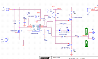
I'm cheking my application with BQ29209 about overvolage protecion condition.

During charge the OUT pin go high at 4295 mV but when the Vbad decrease of 20/30mV the OUT pin go low; in the data sheet is showed an hysteresis min of 200mV.

It is wrong the data sheet ?

Thank You 

Best Regards

Stefano 

  • Hello Stefano,

    I've tested on our board before (When I confirmed that OVP disabled cell balancing) and found the OV hysteresis was accurate to the datasheet spec (~300-mV). I would trigger OVP at ~4.3-V and it recovered (OUT low) at ~4.0-V.

    Do you see this on a different part? Are you measuring directly at the input pins?

    Best Regards,

    Luis Hernandez Salomon

  • Hi Luis,

     I read on the top of the component:

    209
    TI 191
    A6DP

    Then I suppose that the component is right and the measure is directly on the input pin

    I've check also on the other PCBA and the result is the same

    BR

    Stefano

  • Hello Stefano,

    Have you tried using other ICs to see if it's the same?

    Could you also describe what is the Q5/Q4 circuit? Can this be affecting the voltage reading somehow?

    Best Regards,

    Luis Hernandez Salomon

  • Hello Luis,

    Could you also describe what is the Q5/Q4 circuit?

    Are the external mos for increasing balance current,R4 is not mounted 

    Have you tried using other ICs to see if it's the same?
    I've check also on the other PCBA and the result is the same
    Can this be affecting the voltage reading somehow?

    The second PCBA checked is without external mos.

    Best Regards

    Stefan o 

  • Hello Stefano,

    I understand the circuit now. I see you tested in another PCB, but did you test using multiple ICs? It would be good to confirm also if they have different markings.

    Could you also describe you're exact testing sequence and how it was measured/tested? I want to try it from my side with our part.

    Best Regards,

    Luis Hernandez Salomon

  • Hello Luis,

     the other IC is marked:
    209
    TI 191
    A5DP

    About the sequence:

    - using 2 batteries with 3650mV and 4250mV 
    - connect the charger that start in CC at 100mA
    - when the higher battery reach 4295mV OUT go high 
    - connect a load directly to the battery with a 50/100mA CC
    - the battery voltage decrease
    - when it reach 4230mV OUT go low

    More simple sequence.

    Best Regards

    Stefano Sivera

  • Hello Stefano,

    Thank you for the sequence!

    I will be checking it out tomorrow and tell you if I see anything different. I apologize for the wait, today I unfortunately did not have time to go through it.

    Meanwhile could you test with a power supply just to make sure all is okay?

    Best Regards,

    Luis Hernandez Salomon

  • Hello Luis,

    Meanwhile could you test with a power supply just to make sure all is okay?

    I don't understand what do you mean.

    Stefano 

  • Hello Stefano,

    I meant that if you could test on your board using power supplies for the cell inputs instead of using real batteries. Then change the power supply voltage to OVP and down to see when it recovers.

    Do this test on the board without the external FETs just to confirm and cell balancing disabled so it does not affect anything.

    I recreated your test sequence in our board with two power supplies and two resistors. I connected 1-kOhm across each cell input, from VC2 to VC1 and VC1 to Vss, and I put a power supply for each in order to adjust their individual voltages. I performed the test in the following ways:

    • Cell balancing ENABLED:
      • VC2 = ~4.235-V, VC1 = ~3.65-V
        • Ramped up VC2 until OVP triggers (~4.3-V). OUT goes HIGH.
        • Lowered VC2 voltage until device recovers (~4.0-V). OUT goes LOW.
      • VC2 = ~3.6-V, VC1 = ~4.235-V.
        • Ramped up VC1 until OVP triggers (~4.3-V). OUT goes HIGH.
        • Lowered VC1 voltage until device recovers (~4.0-V). OUT goes LOW.
    • Cell Balancing DISABLED:
      • VC2 = ~4.235-V, VC1 = ~3.65-V
        • Ramped up VC2 until OVP triggers (~4.3-V). OUT goes HIGH.
        • Lowered VC2 voltage until device recovers (~4.0-V). OUT goes LOW.
      • VC2 = ~3.6-V, VC1 = ~4.235-V.
        • Ramped up VC1 until OVP triggers (~4.3-V). OUT goes HIGH.
        • Lowered VC1 voltage until device recovers (~4.0-V). OUT goes LOW.

    In all cases I saw the hysteresis working as intended.

    Best Regards,

    Luis Hernandez Salomon

  • Hello Luis, understood about power supply, I doing the test and effectively in this way the hyst. is 300mV. I fon't understand what changes with the battery, I have also verify with the scope  and there is not transition voltage on the real battery.

    Best Regards

    Stefano 

  • Hello Stefano,

    Could you try adding large capacitors across the battery cells and charge/discharge the battery? It could be that when you apply a load the voltage of the cell is dipping enough to get out of OVP.

    Best Regards,

    Luis Hernandez Salomon