This thread has been locked.

If you have a related question, please click the "Ask a related question" button in the top right corner. The newly created question will be automatically linked to this question.

TPS2HB50-Q1: Output is duty cycled

Part Number: TPS2HB50-Q1

Hello,

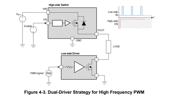
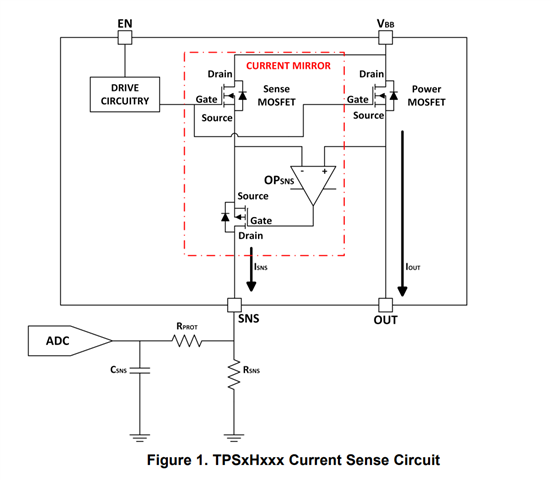
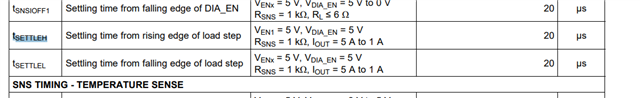
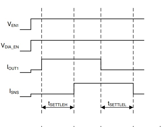
I have a question. what is happening when I have on the output a load and then an additonal MOSFET connected to ground to generate a PWM signal. The PWM frequency of the MOSFET is 3kHz. What does it mean for the current measurement inside the IC. Which value do I get on the SNS output, measuring the current?. Which value on ILIM I  have to set? The duty cycle can be in the range of 50% to 100%.

Thanks a lot!

Best regards, Xaver  

  • Xaver,

    3Khz is going to be too fast for the slew/rate and turn-on/turn-off delay for our high-side switches. You are going to see distortion on the output as the high-side switch will not be able to keep up with the switching. Generally our high-side switches are topped out at 1Khz with a 50% duty cycle. For more information you can see the following application note:

    https://www.ti.com/lit/pdf/slvaf10

    To support higher switching frequencies, it is recommended to have a low-side switch in combination with the high-side switch and do the switching on the low side:

  • Hello,

    as already Mr. Xaver has written we already have this combination as you have described. The 3 kHz PWM are given on the Low Side Fet. The HS Switch acts as a safety switch and is permanently switched on. The question is how does the current measurement from the HS Switch behave? How is the sampling rate of the HS current measurement, filter times. We do not find this information in the data sheet. Thank you

    Best regards,

    Daniel

  • Daniel,

    I understand the question now- sorry for my misunderstanding.

    The way that the current sense works is that it is based off a current mirror- so the feedback that is getting reported via the SNS pin is essentially there in real time. Conceptually, you can see the circuitry internal to the device here:

    (it says Hxxx, but it is the same for HBxx).

    In the datasheet, two important parameters to look at are tsettleH and tsettleL:

    This will essentially give you the latency required to sense the change in current on the SNS output versus a change in the actual load current. It is important to note that regardless of what is reported by the SNS pin and the latencies, the device is designed not to fail in events like overcurrent, short-to-ground, thermal events, etc. 

    The following application note goes into more of the intimate detail with out the current sensing circuitry works:
    https://www.ti.com/lit/SLVAE08