This thread has been locked.

If you have a related question, please click the "Ask a related question" button in the top right corner. The newly created question will be automatically linked to this question.

TPS650861: After configure program mode, can't control each power output by CTL pin.

Part Number: TPS650861
Other Parts Discussed in Thread: IPG-UI

Hi,

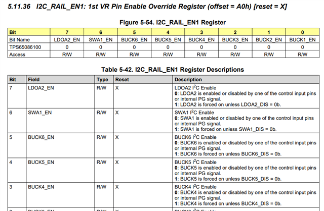
I am trying to control power on sequence for CPU with CTL pin, after configuring program mode in address 0X38, but it didn't output correctly. In the end, we found also a need to configure register 0XA0 each to high in address 0X5E, then allow control power output by CTL pin. According to the datasheet described register 0XA0 should configure each to low, then can control power output by CTL pin. Am I missing some detail?  

  • Hi Shih,

    For programming / testing of the TPS650861, we highly recommend the BOOSTXL-TPS650861. This evaluation board allows you to program the TPS650861 using our OTP Generator document and IPG-UI software. 

    BOOSTXL-TPS650861 EVM User’s Guide

    TPS65086100 OTP Generator (Rev. D)

    In regards to your current question, there are a few steps to debug the programming process:

    1) Can you enable and disable power rails manually using REG 0xA0? Make sure that you can successfully change register setting in address 0x5E without issues (try changing the BUCK4 output voltage using REG 0x92 bits[7:1]). Read back the values after a write to confirm a successful command. A power cycle will cause all registers to reset to default values.

    2) You will not be able to read or write any 0x38 registers until you apply 7V on CTL4. Once 7V is applied at CTL4, I recommend setting REG 0x02 bit[7] = 1 in order to keep the TPS650861 in programming mode. Once this is done, you may remove the 7V from CTL4 and you should still have access to registers in the 0x38 address. A power cycle will take the device out of programming mode.

    3) While in programming mode you may change register settings as desired.

    • In order to control power outputs with the CTLx pins, bits in REG 0xA0 and REG 0xA1 need to be set to 0 for each power output you want to control with CTLx.
    • Power rails can be assigned to a CTLx pin using the registers in address 0x38. For example, BUCK4 enable can be assigned to CTL1 by setting REG 0x11 bits[4:2] = 000. The other power rails are controlled similarly. See Section 5.12 in the datasheet for a full list of 0x38 registers.
    • These register settings will be reset after a power cycle unless you continue with the OTP burning process as detailed in the TPS65086100 Non-Volatile Memory Programming Guide Section 6.

    Regards,

    James