This thread has been locked.

If you have a related question, please click the "Ask a related question" button in the top right corner. The newly created question will be automatically linked to this question.

LMG3422R030: Half-bridge PCB Layout & Schematic Review

Part Number: LMG3422R030
Other Parts Discussed in Thread: ISO7731,

Hello,

I would like to request a review for the design of a half-bridge board at a desired switching frequency of 500 kHz and output maximum power of 500 W at 8-ohm loudspeaker for a class D audio power amplifier.

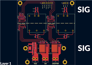
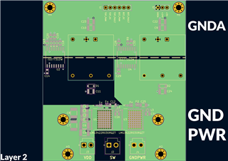
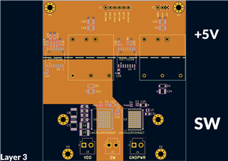
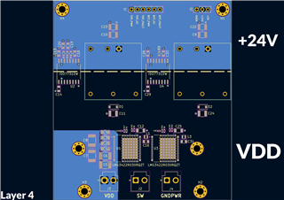
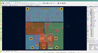
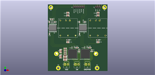
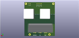
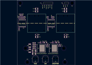
The PCB consists of four layers, with each layer labeled in the figures attached.

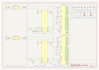
Each copper layer is 1 oz thickness, with board thickness of 1.6 mm. The design requires the use of two isolated DC-DC converters (TRACO POWER - THL 15-2412WI) as well as two digital isolators (ISO7731). Due to that, the board is divided across the middle into two separate sections.

The temperature pin (TEMP) of the switching devices is intentionally ignored in the PCB design.

Attached below are the pictures for each layer, and the complete half-bridge schematic.
 4846.Schematic.pdf
Thank you.

  • Hi Imad,

    We should have a response next week.

    Thanks,

    Travis

  • Hi Imad,

    Apologies for the late response. I can review the LMG3422R030, but I am not qualified to review the ISO7731DW. That being said, I don't see anything with the isolator that would cause an issue. You can create an E2E thread with ISO7731 as the part in question to have it reviewed by someone qualified if desired.

    Here's my comments:

    1. PS1: Consider adding common mode choke to output.

    2. Layers 2 & 3: Try to avoid overlapping SW node & GND when possible, adds switch node capacitance. Some amount of overlap is unavoidable.

    3. Layers 1 & 2: Try to avoid running high-side signals over ground, there can be significant interference when switching. Run them over SW instead.

    4. Layer 3: The large SW node plane will likely become a major EMI radiator. Given your application is for university research, this might not be a problem.

    5. Layers 2 & 4: We generally recommend placing the ground and vdd planes on adjacent layers to reduce power loop inductance and ringing. That being said, your application has over 400V of FET margin, so I doubt this will be a problem.

    Thanks,

    Travis

  • Thank you Mr.Travis for the reply, unfortunately that the PCB has been fabricated already, the GND plane overlap with SW plane has been minimized even further.

    Unfortunately I didn't add a choke inductor to the output, is that a problem?

    Thank you!

  • Hi Imad,

    The concern is from common mode current through the isolation capacitance of the power supply. I can't confirm if it will be a problem for your application.

    Thanks,

    Travis