This thread has been locked.

If you have a related question, please click the "Ask a related question" button in the top right corner. The newly created question will be automatically linked to this question.

LM5022: LM5022 design issue

Part Number: LM5022
Other Parts Discussed in Thread: PMP20497, TPS23754

Hi Sir,

The power board function is 54 V transfer to 12V output voltage.

There have 5pcs PCBA that can't generate 12V output normally. After analysis , the LM5022 is broke such  it can't generate 12V output. 

Rework new LM5022 , they can generate 12output normally.

The transformer part number is RM6-136 an mosfet part number is MTE65N20H8.

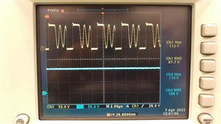
Attached is the test result , please help to confirm whether the waveform  for Vin, Vcc of LM5022 and Vds of mosfet are normally or not

thanks

  • Hi Fang,

    Thanks for sending a detailed test report.

    When looking at the waveform of Vin and VCC, there is a strong voltage spike of Vin during startup which seems to go up to 66.8V.
    This is above the abs max ratings of the device, so even if it only occurs for a short period of time, it can be enough to permanently damage the device.
    Please make sure to never exceed any abs max limits, as I assume this is the source of the device failure.

    To reduce the Vin overshoot at startup, you can try to increase the capacitance at the VIN pin and check if the overshoot becomes smaller.

    The measurements on the MOSFET look good to me, but the ratings of the diode D10 seem to be exceeded as well.
    For this, I would recommend to either replace the diode, or recalculate the RCD snubber design.
    We provide a tool called Power Stage Designer, which comes with a helpful feature of calculating RCD snubbers for flyback topology.
    You can download the tool from here:
    https://www.ti.com/tool/POWERSTAGE-DESIGNER

    Please let me know if you have additional questions.

    Best regards,
    Niklas

  • Hi Sir,

    Attached is the test result  for LM5022 Vin amd Mosfet Vds during startup and shutdown. Please refer to the related sheet.

    Would you help to advise the capacitance value we should increase at the VIN pin? Then ,we ca check if the Vin overshoot result at startup.

    thanksWRGAX28_1A1G power board issue20230407.xlsx

  • Hi Sir,

    Regarding diode D10 voltage level issue , we retest and change the scope voltage scale to 50V  for comparison.

    The channel1 is postive and channel2 is negaive.The result shows about 3~5V difference in measurement, please refer to acched pictures.

    How about correct D10  postive and  negaive voltage level? Please advise

    thanks

  • Hello sherman,

    The abs max rating of the LM5022 is 65V and the device can get damaged if the voltage on the VIN pin gets higher than this. At startup the measurements show a high overshoot on the 54V input voltage measurement and if this overshoot is applied to LM5022 it can get damaged. You can increase the capacitance on the VIN pin as high as needed to filter the startup overshoot.

    I do not understand the measurement in the scope plot above. Please explain what exactly you measured there.

    Best regards,

    Brigitte

  • Hi Sir,

    Regarding diode D10 voltage test, attached is the measurement explanation for detail.Please help to check that and advise

    thanksDiode_D10 _test_explanation20230410.pptx

  • Hi Sherman,

    The voltage stress of D10 is more than 100V. 200V diode such as ES1D is suggested.

    VIN over voltage should be the reason why BLM5022 is damaged.

    Best Regards,

    Feng Ji

  • Hi Sir,

    We have below questions, please help to advise

    1. From the schematic of previous excel file, did you mean increase the capacitance C32 value at the VIN pin to check if the overshoot becomes smaller?

    2. If the Vin input level for LM5022 pin1(Vin) is larger  , is it caused LM5022 pin4(Vcc) damage directly? Please help to comment.

    3.Please help to comment whether the transformer T1 specification is appropriate in this design.

    thanks

  • Hi Brigitte,Feng,

    We have some questions regarding LM5022 IC pin name Vcc (number 4) function.

    From LM5022 datasheet , we find it has two version. One shows December/2017 released, the other shows July/2020 released.Please refer to attached file.We refer to TI PMP20497 design to implement our LM5022 design.

    We find pin name Vcc (number 4)  is defined to an output. The function shows Output of the internal, high-voltage linear regulator: This pin must be bypassed to the GND pin with a ceramic capacitor.  According to some TPS23754  POE flyback design structure experience, in general ,there has a transformer with AUX to proivde a fixed voltage level for Vcc. And Vcc shows an bias function for controller IC inernal regulator and is defined to an input. From TI PMP20497 design , the transformer has AUX that is similar to POE flyback concept.LM5022 _Vcc_question20230413.pptx Would you help to explain more regarding  LM5022 Vcc idefimed to an output reason?

    thanks

  • Hi Shermen,

    1. Make sure VIN less than 65V at any time. Increase C32 may help. 

    2. We cannot say VIN overvoltage will lead to VCC damage.

    3. What is your concern about T1? And I can find datasheet of T1, while RM6-136 is only the core part number.

    Best Regards,

    Feng Ji

  • Hi Feng,

    Reattached T1 transformer RM6-136 datasheet. We refer TI PMP20497 design to have our design.

    Since we adopt RM6-136  in our design , so we'd like to know if this part specification is appropriate in LM5022 design.

    please advise

    thanksSPEC-RM6-136-B.pdf

  • Hi Shermen,

    VCC is the output of the internal voltage regulator. You can also apply 7.5-14V voltage externally to VCC.

    7.3.1 High-Voltage Start-Up Regulator in the datasheet describe:

    In applications using a transformer, an auxiliary winding can be connected through a diode to the VCC pin. This winding must raise the VCC pin voltage to above 7.5 V to shut off the internal start-up regulator. Powering VCC from an auxiliary winding improves conversion efficiency while reducing the power dissipated in the controller.

    Best Regards,

    Feng Ji

  • Feng, 

    So far the damaged all happened at Vcc not Vin, does it make sense the root cause happened at Vin? 

    Regards,

    Allan

  • Hi Allan,

    How did you determine "damaged all happened at Vcc not Vin". If VCC is short to GND, you should also check if VCC goes above 14V during operation.

    Best Regards,

    Feng Ji