This thread has been locked.

If you have a related question, please click the "Ask a related question" button in the top right corner. The newly created question will be automatically linked to this question.

TPS62162 :Unstable output current

Part Number: TPS62162

Hello everyone,
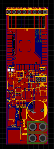
I am currently on a project to create a PCB with esp32.
Except that problem, I solder everything well, all the tracks are good, I changed the dc down (tps62162), but nothing helped.
If I supply my PCB with 6v, the PCB works without any problems and the esp32 starts.
If I supply my PCB with a voltage greater than 6v the esp42 does not start and the voltage at the terminal is less than 3v.
I changed the esp several times, I changed the dc-down.
When I connect a development esp32 in bypass it does not work either.
Not having an oscilloscope, I plugged a white led of 3.2v on 2 pins of the PCB to see (Yeah it looks stupid like that), the led flashes as if the TPS62162 restarts infinitely, I therefore think that the output voltage is not stable and the voltmeter does not detect it.
Now that I know the problem, I tried to look for where it could come from .. but I still can't find ..
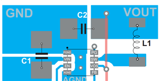
For the regulator connection see the diagram below.

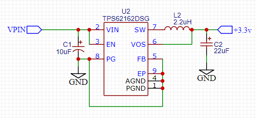
I use VLCF4020T-2R2N1R7 inductor has L2

Thank you.

  • If you ever think that the problem can come from the pcb here is an image of it :

  • Hi Guillaume,

    What does ESP32/42 here mean?

    The schematic looks good.

    It look like the device runs into hiccup mode somehow. I think there're two possible reasons.

    It would be better if you have a oscilloscope to test the waveform of Vin/EN, SW and VOS.

    1. The load current is higher with the Vin increases and the device run into current limit performance. Please try to disconnect the load and try again.

    2. The loop is extremely unstable due to poor external component/layout.  Please send me the layout file through email (athos-zhao@ti.com) if possible. Or at lease the screenshot of VOS, AGND trace.

  • Hi Athos, esp32 is this precisely.

    the maximum current of the esp32 is less than 1A.
    I send you all the documents.

    Thank you very much.

  • Hi Guilaume,

    The layout is indeed poor for this case, which may cause the unstable loop.

    Please follow the layout guidelines of datasheet.

    1. There should be polygon of Vin, PGND, SW, VOUT but not just connected by traces. Especially PGND, you can see your PGND net are arranged mess on t the board with thin traces.

    2. Input capacitor should be directly connected to Vin pin not EN pin.

    3. VOS is a sensitive node and it should connect in the shortest way to VOUT at the output capacitor. As it carries information about the output voltage, it should be connected as close as possible to the actual output voltage (at the output capacitor). You should neither connect many VOUT points at VOS pin, nor lay power trace through VOS.

  • Hi Athos,
    Thank for your help, i did not think it was so important !
    I remake my pcb,it's difficult because of the size constraints of my pcb.
    i have one question it is possible to pass vos under L1 like this ? 
    I send you on your email, all pcb, if you need.
    Thank.

  • Hi Guilaume,

    We don't recommend this because VOS is a sensitive node which should not be traced nearby high dv/dt signal like SW.

  • Thank you Athos !