This thread has been locked.

If you have a related question, please click the "Ask a related question" button in the top right corner. The newly created question will be automatically linked to this question.

UCC27322: PGND and SGND layout connections with UCC27322

Part Number: UCC27322

Good morning,

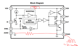
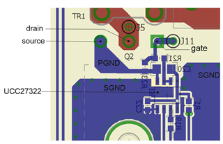
the UCC27322 circuit in SO-8 version has 2 pins for PGND and SGND.
What do you recommend for the connection of these 2 pins on the PCB?
In my opinion, it is necessary to connect PGND directly and as short as possible to the source of the MOS and SGND to the ground plane of the control signals, but where to connect the common point of these 2 GNDs for a low noise and best practice?

I am attaching the part of the driver schematic concerned and the 2 possibilities for connecting the GNDs (pin 4 and 5), thank you in advance for your advice.

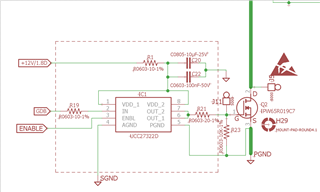
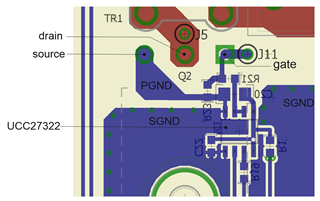
Red layer is top layer, blue is bottom layer, the UCC27322 is in bottom layer

Best regards.

JY

  • Hello JY,

    Have you read the layout section of the datasheet?

    The guidance in here is to connect the two grounds with a single trace, so image 1 is closer to this description. This trace will act somewhat like a high-pass filter. The section also has guidance for other techniques that can be used depending on noise. With a 20Ω gate resistor, I think you will probably not need to implement some of these advanced noise techniques. This is because the di/dt in your switching loop should be fairly small and therefore not very noisy. It is up to you and your system though.

    Thanks,

    Alex M.

  • Hello Alex,

    Yes of course I read the datasheet as I suppose any good professional here.

    But if I ask the question on the forum it is precisely because I did not find a satisfactory answer there.
    A high pass filter? I rather see it as a low pass filter, can you tell me how it is a high pass filter?
    My PFC is several kW and the di/dt are precisely my problem because I am trying to make a double-sided PCB in a new version and this imposes strong constraints on me in terms of placement where I am confronted with significant noises which strongly disrupt my command lines.
    Currently I am connected as indicated on the datasheet with SGND to PGND directly as the drawing but it does not work well, my PFC is interlaced it amounts to having 2 connections of the ground plane signals on 2 noisy masses and I do not find not that very wise.
    I thought that the PGND should be separated from the SGND to precisely dissociate the switching noises.

    Regards.

    JY

  • Hello JY,

    Sorry, high-pass was a mistake, a series inductor should be low-pass. If the PCB version with the two grounds connected is having noise issues, then I agree that the best option will be to separate them and work from there. If you separate the VDD and GND pins, you have a situation like this:

    So you need to meet a few conditions:

    1. AGND and PGND need low Z connection for DC and any input signal frequency.
    2. AGND and PGND need high Z connection for noise frequency.
    3. There should be no easy path for the noise to travel through OUT pins (note body diodes in pullup/pulldown, also when the driver pulls high there is connection to VDD).
    4. These circuits should not impede the turn-on or turn-off loop of the driver.

    Generally noise issues like this can be extremely tricky, and many people have their own preferred methods. Personally, I like ferrite beads. Since you already have a board and know the noise frequency, you can select a ferrite bead that blocks the target frequency and insert that between AGND and PGND, possibly the VDDs, and also in the gate drive loop to block OUT. I have spent some time simulating this and this was the best I managed:

    The green is a constant 100MHZ noise on PGND (unrealistic, but helps stress test solution) and red is AGND. This is using series inductances between the VDD pins and GND pins. Of course, it is always difficult to simulate noise issues like this accurately. The other options such as the antiparallel diodes can also help. To avoid doing a bunch of board spins, I would definitely separate the pins in question, and use placeholder footprints to evaluate different solutions. Please let me know if you have any follow-up questions.

    Thanks,

    Alex M.

  • Ok Alex, 

    I'll give it a try and let you know my results.
    Thank you for your time and advice.

    Regards.

    JY

  • Hello JY,

    No problem. Feel free to reply to this thread with results. I'm curious what solution will work the best.

    Thanks,

    Alex M.