This thread has been locked.

If you have a related question, please click the "Ask a related question" button in the top right corner. The newly created question will be automatically linked to this question.

LM61460-Q1: Some questions about chip spread spectrum

Part Number: LM61460-Q1

Hi team,

My customer has some questions about chip spread spectrum, I hope I can help to answer them quickly:

1、The spread spectrum function of Auto mode is turned off in the light-load frequency reduction mode, and it is automatically turned on above the medium load. What kind of detection mechanism is this spread spectrum? What is the internal sense of the chip?

2、How does the chip itself judge that the load is above the medium load? How to judge the need for frequency spreading? Is Auto mode the same as FPWM?

Thanks!

  • Hello,

    1.The datasheet only provides description on when the SPSP function is disabled and it sounds like customer is interested in understanding more about bullet point #2. Are you asking specifically what the detection block of the auto mode looks like? From datasheet description, once the device is in light load auto mode condition, it would turn off the spread spectrum circuitry. 

    2. The device operates in CCM (continuous conduction mode) with fixed switching frequency when load current is above half the inductor ripple current. FPWM is fixed pulse width modulation and it is a condition where the switching frequency is always fixed and square wave even at lighter loads. If there is enough load current, it will be in "medium load" enough to be in CCM condition. FPWM is not the same as Auto mode at light load.  

    Active mode is described in Section 9.4.3. Note that at light load the device will be in PFM (pulse frequency modulation) which will help with improving efficiency. In Active mode there is an auto-mode feature that is split between diode emulation and frequency reduction. More details can be read in the datasheet. The high level is that at lighter loads in Active mode the device will be in diode emulation where the inductor current will never fall below zero. As load current is reduced, the time it takes the inductor current to ramp down to zero takes longer which in turn reduces the switching of the device to maintain output regulation. 

    Regards,

    Jimmy

  • Hi Jimmy,

    Thanks for your reply!

    My customer have another question.

    May I ask if you have used EVM to test the change of the output when the input is suddenly lower than the minimum input voltage. The customer's current output voltage is 4V and 3.3V, and the minimum input voltage is 3.95V. How does the output voltage of the subsequent stage change when the VIN voltage suddenly drops below the minimum input?


    Is it linearly reduced? or suddenly the cutoff drops to 0?

  • Hi,

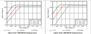
    Below is the dropout behavior for 3.3V output that is also in the datasheet. The point where the slope of the curves is called the dropout point. 

    As Vin is decreased, it will get enter the dropout point and start linearly scaling output voltage down. 

    Generally in dropout condition the output voltage will be approximately the input voltage minus a diode drop.

    Regards,

    Jimmy