This thread has been locked.

If you have a related question, please click the "Ask a related question" button in the top right corner. The newly created question will be automatically linked to this question.

TPS6594-Q1: TPS6594-Q1 question consultation

Part Number: TPS6594-Q1

Hi  engineer: 

      About  TPS6594-Q1

     EQ1:The data sheet mentions: "Current through input protection FET: Between VSYS_SENSE & VCCA should be lower than 15A", can you describe the detection mechanism of the input current overcurrent protection in detail?

       EQ2:In the multi-PMIC synchronization state, how to analyze the fault code transmitted by the Secondary PMIC through SPMI from the I2C2 communication transmitted from the Primary PMIC to the MCU?

       EQ3:What are the I2C1_ID and I2C2_ID of the three materials TPS6594C41-Q1, TPS6594C31-Q1 and TPS6594133A-Q1? 

       EQ4:If the output ports of LDO1~LDO4 pins are used as external voltage monitoring, what is the output current threshold to start over-current shutdown? And is the threshold configurable?

       EQ5:Can TPS6594-Q1 read the specific values of input and output voltage and input and output current, and feed back the specific values to the MCU through I2C2?(Instead of just feeding back a fault interrupt signal through I2C when the input and output current or voltage range is outside the threshold range.)

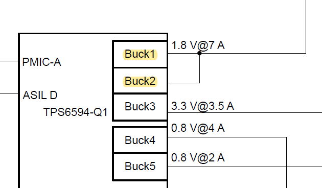
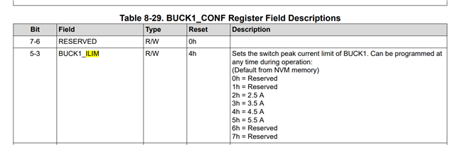
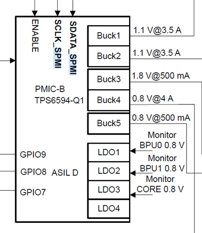
       EQ6:As shown below: BUCK1 and BUCK2 in multiphase configurations,can the overcurrent monitoring threshold reach 7A?
The register configuration in the data sheet seems to be only from 2.5A up to 5.5A for a single channel. The combination of the two BUCKs becomes a multi-phase adjustment mode. Will the over-current interrupt protection be triggered if the current reaches 6.5A?Is it convenient to give a description of the ILIM protection mechanism?


  • EQ2:In the multi-PMIC synchronization state, how to analyze the fault code transmitted by the Secondary PMIC through SPMI from the I2C2 communication transmitted from the Primary PMIC to the MCU?

    In a multi-PMIC solution, you must communicate with the secondary PMICs via I2C1 to read the faults. I2C2 is for Watchdog communication. 

    EQ3:What are the I2C1_ID and I2C2_ID of the three materials TPS6594C41-Q1, TPS6594C31-Q1 and TPS6594133A-Q1? 

    TPS6594C41 and TPS6594C31  should be TPS6594C401 and TPS6594C301 respectively.

    TPS6594C301:  I2C1_ID = 0x48, I2C2_ID = 0x12

    TPS6594C401:  I2C1_ID = 0x4C, I2C2_ID =0x13

    TPS6594133A:  I2C1_ID = 0x48, I2C2_ID = 0x12

    EQ4:If the output ports of LDO1~LDO4 pins are used as external voltage monitoring, what is the output current threshold to start over-current shutdown? And is the threshold configurable?

    LDO1-LDO4 monitor voltage only. The over current protection comes from the discrete buck converters themselves. TPS6287x in this case has over current protection. The PMICs do take the PGOODs of these bucks and react if they indicate a fault besides output voltage.

    EQ5:Can TPS6594-Q1 read the specific values of input and output voltage and input and output current, and feed back the specific values to the MCU through I2C2?(Instead of just feeding back a fault interrupt signal through I2C when the input and output current or voltage range is outside the threshold range.)

    The TPS6594 PMIC does not have this feature.

    The register configuration in the data sheet seems to be only from 2.5A up to 5.5A for a single channel. The combination of the two BUCKs becomes a multi-phase adjustment mode. Will the over-current interrupt protection be triggered if the current reaches 6.5A?

    The ILIM listed in the BUCKx_CONF register per phase switch current. When operating correctly in multi-phase mode, the BUCKs will distribute the current amongst the phases evenly. For example, at 6.5A of load there would be 3.25A in BUCK1 and 3.25A in BUCK2.

    EQ1:The data sheet mentions: "Current through input protection FET: Between VSYS_SENSE & VCCA should be lower than 15A", can you describe the detection mechanism of the input current overcurrent protection in detail?

    I will confer with my colleagues and get back to you on this question.

  • Closing the loop on this question...

    EQ1:The data sheet mentions: "Current through input protection FET: Between VSYS_SENSE & VCCA should be lower than 15A", can you describe the detection mechanism of the input current overcurrent protection in detail?

    In regards to the 15A max operating current:

    • The PMIC does NOT monitor the current through the safety FET.
    • For a 3.3V input system OVPGDRV will be ~9V while on a 5V system, OPGDRV will be ~11.5V. This impacts FET RDSon.
    • The 15A mentioned the data sheet are based on recommend Safety FET listed in the application section of the data sheet and estimated RDSon over the OVPGDRV voltage range.
    • Customer is free to go above 15A  as long as VCCA voltage stays within OV/UV voltage monitoring window and the power-FET operates within its specified safe-operating-area
    • The gate-capacitance of the chosen power-FET should not exceed the max value of 4nF given in parameter #9.11 (C_iss_extFET) in datasheet section 7.13. A higher gate-capacitance will cause the PMIC to no longer satisfy the specified latency times after OVP detection at the VSYS_SENSE pin and the VCCA pin. These latency times are specified in parameters #26.2 (t_latency_VSYSOVP) and #26.3a/b (t_latency_VCCAOVP). If the PMIC cannot satisfy these specified latency times, the voltage at the VCCA, PVIN_Bx and PVIN_LDOx pins can during an over-voltage event at the PMIC input supply violate the abs. max rating as specified in footnote (3) of parameters M1.3, M1.4 and M1.7