This thread has been locked.

If you have a related question, please click the "Ask a related question" button in the top right corner. The newly created question will be automatically linked to this question.

UC1846: sepic control using TINA TI

Part Number: UC1846
Other Parts Discussed in Thread: TLV3501

Hello:

I can make the TINA model work using UC1846 for a SEPIC converter but it is not giving correct results.

The grand scheme here is to explore how it will work with feedback and then optimize the L & C values. 

I suspect I have all the wrong semiconductors- it is almost impossible to guess what to select from TINA TI list of devices. 

If I can email you the model, is it possible to help select proper devices from some list you might have that are more convenient to choose from?

Or use some artifact to make it work?

Any help will be appreciated.

r

  • Robin,

    Thanks for connecting through E2E - can you upload to E2E, the TINA model of the SPEIC you are tying to simulate?

    Regards,

    Steve

  • Hello Steve:

    I am attaching the file "as-is"...I will add some notes on things that are obviously different from the UC1868 example in TINA TI.

    -Note1: SEPIC DCM PFC topology is almost a double SEPIC when it is used in the "Bridgelesss" case. SO you see 2 inductors, 2 capacitors, and one combined output summing inductor.

    Note2: switches need to have a reverse blocking feature. This is done by the diodes. Although in theory, one can use GaN- not worth it due to the complexity of GaN drive schemes vendors impose.

    -Note3: although a lot of people say "You can drive the switches with 1 PWM", in reality, that is not true: because the switch nodes can have decaying +ve voltage when it is not supposed to switch. That means conduction at a wrong time. This is reason for "gating" the PWM from UC1846 so that a switch is OFF during half the line period when it is not supposed to switch. The gating signal is derived by the TLV3501  comparator.

    Rest is fairly straightforward.

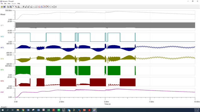
    One thing troubling me is that for whatever Options I selected, it takes a lot of time. After getting to the "regulation " range output, it crashes. 

    The goal is to understand load/line regulation, step load response, optimize inductor-capacitor values, coupled inductor instead of 3 inductors, and transformer isolation which will permit SR using HV GaN from GAnSystems devices- which requires careful extraction of SR gate timing. No SR controller can be used due to HV involved.

    Any comment to ameliorate the model will be highly appreciated.

    r

    UC1846_TRANS_frdn2ctrl.TSC

  • Robin,

    "One thing troubling me is that for whatever Options I selected, it takes a lot of time. After getting to the "regulation " range output, it crashes. "

    I ran the sim you sent. Yes, it runs slow and takes a long time to complete but it did run without errors of convergence issues. Regarding your simulation crash error, I would recommend to try setting initial conditions on capacitors and inductors. A previous E2E thread here mentions how to do this in TINA. I have not personally analyzed, simulated or designed a PFC SEPIC, though the idea seems to be entrenched in Unitrode/TI legacy....Lloyd Dixon Seminar Topic here.

    Regards,

    Steve