This thread has been locked.

If you have a related question, please click the "Ask a related question" button in the top right corner. The newly created question will be automatically linked to this question.

UCC28700: Aux winding and Vcc question

Expert 1035 points
Part Number: UCC28700

Hi TI experts,

I have a question about UCC28700.

1. Why the VDD connect to VBLK and Vaux. what's Vcc power up sequence?

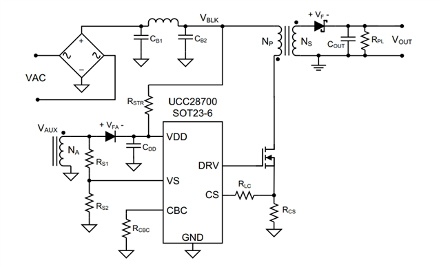
2. Why we need to use this diode? what's the function of this diode? can we remove it?

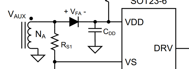
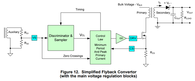
3.What is discriminator and sampler? is this made by analog or digital circuit?

  • Hi,

    1 VDD  connect to VBLK through a resistor to provide initial startup current but after initial start power on, the current to VDD becomes much higher so to avoid high power losses the resistor value is high and not able to maintain VDD required bias current then this is resolved by the Vaud.

    2 the diode is to rectifying the voltage from aux to dc which is required by VDD.

    3 Discriminator is an analog circuit to help sensing and filtering the VS signal to determine Vout and several other monitored parameters. The datasheet page 13 has detailed sensing description.

  • Hi Hong,

    Please see my below comments,

    1. After the power on the Vblk doesn't provide the current to Vdd, do you meant that?

    2. the diode is conducted only when the switch turn off, how about turn on? how to make sure this diode can always turn on?

    3. About Discriminator, I am still confused about how to work, do you have more clear figure about this circuit?

    thanks

  • Hi,

    1. After power on if bias through a resistor to Vbulk the associated power losses are much higher than through the aux winding. So a design is made to bias from the aux and the resistor current small not sufficient to bias the ic.

    2. when Vaux polarity as show by the dot is positive the diode will turn on to conduct, when that dot is negative then the diode off.

    3. The description on page 13 and 14 is for the mechanism of how the discriminator to work. Please describe where you feel need to get additional explanation based on figure 13 to 15

  • Hi Hong,

    1. Got it.

    2. I mean if the dot is negative then the diode off, when the diode off how to provide the power to VDD? Because you said Vbulk can't supply enough current to Vdd.

    3. Could you please tell me what does Discriminator looks like in the analog circuit? This is my first time using this IC so I  am not familiar with Discriminator.. 

    I don't see the Discriminator in the block diagram.

    4. Do you have the SIMPLIS simulation file? I only find the SPICE, but I only can use SIMPLIS

    Jack

  • Hi,

    2. When the diode off, the CDD stored energy will bias the IC. CDD is charged up when the diode is on.

    3. The best way to understand the discriminator is to understand Fig 13 to Fig 15 in the datasheet for you to use the IC. No matter what, you would have to first understand the three figures in order to know how the ic works.

    The discriminator is based on analog although it is easier to describe it using some digital terminology.

    4. The IC has both TINA and Spice so you can use either. Both software to run TINA or PSpice are free to use and free download from ti.com. 

  • Hi Hong,

    2. I got it.

    4. I got it.

    3. As my understanding, when the Is current is zero, the IC can detect the the winding voltage without considering the second side effect.

    but according to Figure 14, how to accurate calculate the TLK reset, Tsmpl, TdM time?

  • Hi,

    TLK is not calculated just set up a blanking time based on the typical application.

    TSMPL is when VS p-p is within certain range 100mV then TSMPL timer starts, and roughly in about 200ns, if VS always within 100mV p-p, then at the end of 200ns, the IC sampler will sample that time instant VS value as the threshold then the discriminator just wait until VS sensed a roll-off compared to the sampled value about 0.5V to 0.75V, then that sampled value is treated as the secondary side output voltage, after compared this voltage to the VS voltage divider to determine next pulse termination threshold (peak current change or fsw change depending on where at the control law fig 15).

    TDM is not calculated but = the above two addition while there is a max TDM about 0.425. If TDM reaches 0.425, then the discriminator will adjust duty cycle each cycle to keep TDM = 0.425 not increase anymore. So this IC can only operate in the DCM to the critical conduction mode (the last DCM before entering continuous conduction mode, CCM).

  • Hello Hong,

    Please see my below comments.

    Are you saying that if the VS voltage remains within 100mV peak-to-peak after 200ns, the voltage at that instant will be sampled, and then there is a waiting period until the VS voltage drops further by approximately 0.5V to 0.75V, at which point the VS voltage is considered as the secondary-side output voltage? Is this understanding correct? If so, why is it necessary to compare this voltage with the VS voltage divider? Isn't this voltage the same as the voltage obtained from the VS voltage divider? Can you provide an example, please?

    Is the reason for not entering CCM mode because the TDM time must always be greater than 0.425?

  • Hi,

    The 100mV is peak to peak. The VS voltage from the divider is the setup for how much regulation achieve, the divider voltage is to compared to the internal reference voltage about 4V to decide if the secondary side output voltage is in regulation.

    TDM max 0.425 is the reason the IC won't operate in CCM. 

  • Hello Hong,

    About your comment, "the discriminator just wait until VS sensed a roll-off compared to the sampled value about 0.5V to 0.75V, then that sampled value is treated as the secondary side output voltage, after compared this voltage to the VS voltage divider to determine next pulse termination threshold"

    1. If VS sample the instant value, why discriminator need to  wait until VS sensed a roll-off compared to the sampled value about 0.5V to 0.75V? why the instant value can't be the secondary side output voltage?

    2."after compared this voltage to the VS voltage divider to determine next pulse termination threshold", in this content, what's difference between this voltage and VS divider voltage? could you please use an example let me understand more easily?

  • Hi,

    1. That is a process to determine the time that TDM ends together with the sampled value for discriminator to decide next cycle operation such as if TDM has reached 0.452, which portion law to use, etc.

    2. Say, if the VS divider value is 3.8V, compared to the internal reference 4V, it means peak current needs to increase, or if peak current already at its max then fsw needs to increase. If VS divider value is 4.1V, then the fsw needs to reduce, or the peak current needs to reduce depending at which portion of the control law (fig 15)

  • Hello Hong,

    Thanks for your help.

    If I have other questions, I will creat a new one.