This thread has been locked.

If you have a related question, please click the "Ask a related question" button in the top right corner. The newly created question will be automatically linked to this question.

TPS22917: TPS22917 VOUT voltage dip

Part Number: TPS22917
Other Parts Discussed in Thread: TPS2116, TPS2117

Hi!

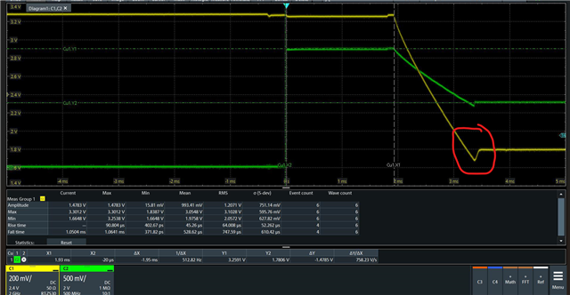
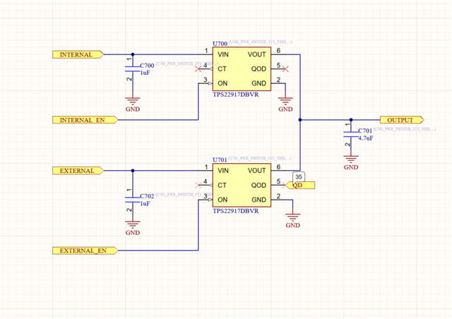
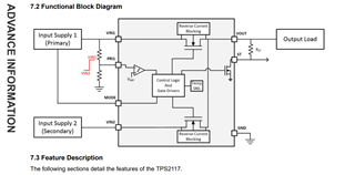
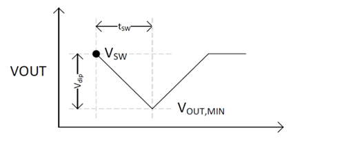
I am using two TPS22917 to switch between internal/external power supply at 2 different levels 1.8V/3.3V.  One TPS22917 is connected to internal buck to generate 1V8. The other one is connected to an external PS that provides 3.3V. The output of both switches are connected together and are used to power VDD on an MCU. We have big capacitors (22uF) at the output (VDD). The problem I have is that when switching from 3V3 external to 1V8 internal we have a dip (brownout) that goes under the reset level of the MCU (1.7V). Why is this happening? My guess is that the reverse current protection gets triggered and blocks the input of the 1V8 until VOUT goes under 1V8 and then it takes a while to re-enable itself giving time to the output capacitors to discharge under the 1.7V but I am not so sure of this looking at the datasheet. Any ideas of what can it be and how to solve it? 
Thanks.

Figure1: Yellow line is VOUT and green line is ON.

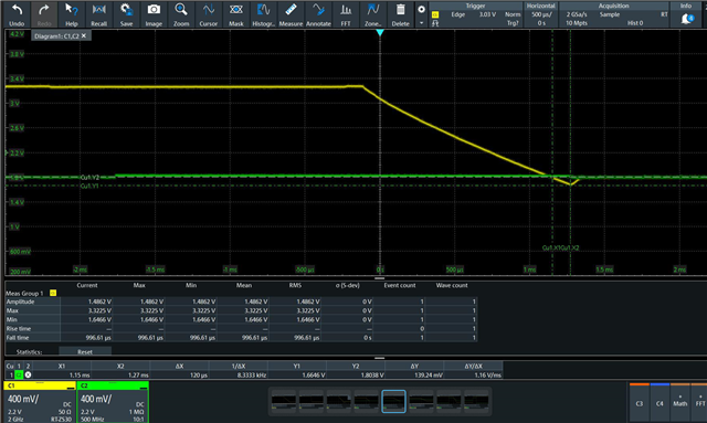
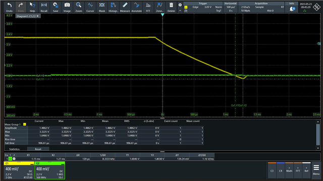
Figure 2: Yellow line is VOUT and green line is the output of the internal buck (1V8).

  • The datasheet states the RCB Activation time to be around 10us. There is no information about the de-activation time and maybe if there is any hysteresis on RCB Release Voltage. Could it be possible to get this information?
    Thanks!

  • Hello,

    My initial thought was the capacitive output load was causing a large enough inrush during loading onto the 1.8V rail the voltage dipped below the 1.7V threshold, in which case additional input capacitance likely would've solved the problem. 

    However, from your second plot, it appears the 1.8V rail is not dipping at all; could you confirm the green line on plot 2 is the exact voltage being sent to the input of the TPS22917? It would also be helpful if you could provide a schematic; the QOD pin is left floating correct? 

    Is there a reason the TPS2116 was not considered? Or the higher current capable TPS2117? These devices are integrated power muxes meant to mux between two supplies within the voltage range 1.6V to 5.5V. 

    With regard to deactivating the switch RCB, the Switch remains off and block reverse current as long as the reverse voltage condition exists. After VOUT has dropped below the VRCB release threshold the device turns back on with slew rate control.

    Best Regards, 

    Elizabeth 

  • Hello Elizabeth,

    Thank you for taking a look at my case. I confirm that the second plot is the exact voltage being sent to the load, so no dipping on that side. I also confirm the QOD is left open in both TPS22917 although we will add this function is the next revision. I am providing the schematic as requested. 

    I will take a look at the TPS22917 and see if it suits our needs. Thanks for the suggestion. 

    Regarding the RCB, do you have numbers for the time it takes to turn back on after VOUT has dropped below the VRCB release?

    I measured in the second plot below and It seems to be around 120us. If this is correct then we can confirm this is the cause for the dip. 

    Thanks!

  • Hello, 

    After VOUT has dropped below the VRCB release threshold (25mV typ), the device turns back on with slew rate control so the delay would be from when Vin>Vout + 25mV typ to when Vout starts increases with slew rate control. 

    I am not finding that parameter anywhere unfortunately, so it very well might be in the realm of 120us. This is around the switchover time we see for our TPS212X power mux devices. I will have to reach out to design to know for sure. 

    In the meantime, if you use the TPS2116, you will see only a 8us voltage drop we refer to as the switchover time. I would recommend using this since your system requires a fast switchover to stay above the 1.6 UVLO of your system. 

    Best Regards, 

    Elizabeth 

  • Hi,

    I am looking at the block diagram of the TPS2116 and it seems like even If I change to this device I might still have the same problem. The RCB blocks will disable the device if I am using different voltage levels, so I will still have a dip that will reset the MCU. Maybe the quick switchover time only applies to situation where you have the same voltage level (like in a backup battery system). Do you think that will be the case?

    Thanks!

  • Hello, 

    Load switches and power muxes are going to power mux differently. 

    In load switches, reverse current has to flow in some amount for it to trigger; this is the same for powerMUX reverse current protection
    The difference is:
    in load switch muxing, you use the reverse current protection to turn off the device during switching
    in pmux muxing, there is a separate switching circuit that handles these cases and protects against the backflow of current by waiting for the output to drop below the input before turning on the channel. so you are not depending on the reverse current protection to turn on and turn off the device. The rev current protection in pmuxes is solely for the event when the channel is ON and is meant to conduct but the output goes high for some fault reason
    in conclusion,
    if you MUX with load switches, you will always see a reverse current flow every time you switch between the inputs; in a power mux, you will not. For power muxes, the voltage drop you will see when you switch between the two supplies will be for only the duration of the tsw time specified in the datasheet. 

    Best Regards, 

    Elizabeth