This thread has been locked.

If you have a related question, please click the "Ask a related question" button in the top right corner. The newly created question will be automatically linked to this question.

TPS40305: BP to BOOT diode damage

Part Number: TPS40305

It looks like the BP to BOOT diode easily gets damaged in my circuit. When the circuit fails, BOOT is no longer charging, but there is still ~6.5V on the BP pin. On a working TPS40305 I measure a 0.68V diode forward voltage from the BP pin to the BOOT pin. On a failing TPS40305 this changed to 0.18V. Does it sound likely that the BOOT diode is damaged?

Webench was used to design a circuit for 20V to 12V at 5A. The same circuit is used for a 15V input and a 20V input. I realize 20V is at the device limit, but I've also seen the TPS40305 BOOT fail when the input voltage is 15V.

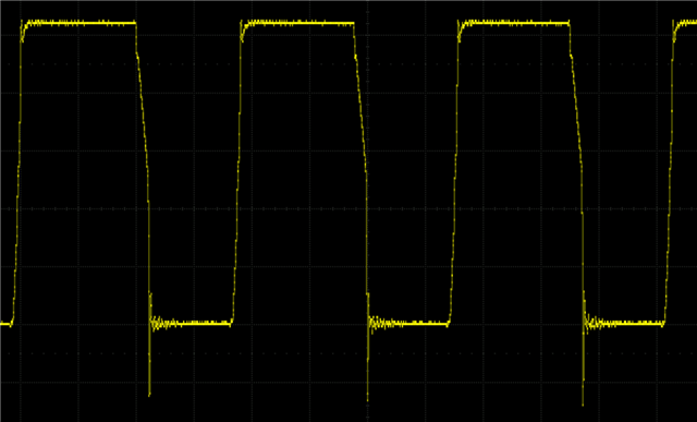
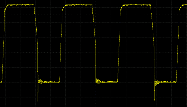
I looked at SW node ringing. I tried a 2.2ohm resistor between the BOOT pin and the boost capacitor. There was some improvement in the ringing after the rising edge, but the ringing after the falling edge was still huge. See plots before and after adding this 2.2ohm resistor:


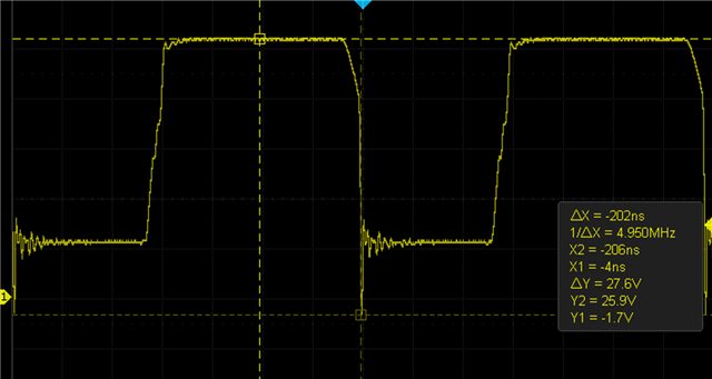
The level on the SW node is dipping below the absolute max rating of -5V. On the BOOT pin I measure levels below the absolute max rating of -0.3V:

Is this a likely cause of the damage? Or could there be other causes? What is the suggested next step to make the circuit reliable?

Thank you,

  •  

    Thank you very much for the question.

    The most common cause of boot-diode failure we have seen with the TPS40305 has has actually been the selection of high-side MOSFETs with too much gate charge resulting in excessive diode current fusing the metal from BP to BOOT open, but that typically causes BOOT to be lower, not closer to BP.  A low reverse impedance from BOOT to BP would be an indication of a "failed short" damage to the BOOT diode.

    When the BP to BOOT metallization fuses open:

    BOOT may charge up very slowly, but HDRV will not rise with BOOT during the turn-on of the high-side FET.  HDRV will instead pull-up to BP.

    This weak pull-up of HDRV will trigger high-side over-current, so the start up of the TPS40305 will contain several very narrow pulses on HDRV and possibly SW, as the high-side short circuit protection limits the on-time.

    After a few pulses, the current limit will shut down switching and time-out for several soft-start periods before trying again.

    If you see that start-up attempt, try added an external BP to BOOT diode.  If the circuit works normally with an external diode, the BP to BOOT metallization has been fused open.

    A negative voltage on switch could cause a high BP to BOOT voltage and induce failure of the BOOT to SW diode.  The negative voltage on SW is induced by the parasitic inductances in the current path for the inductor current resonating with the parasitic capacitance of the switching node after the high-side FET turns off and the low-side FET turns on.  Since the turn-off of the high-side FET draws current out of the gate into HDRV, out SW and back to the source of the high-side MOSFET, the BOOT pin is not involved, so adding a boot resistor does not help.

    The best way to reduce ringing is with a tight switching layout that minimizes the path of the dynamic currents that need to change paths between the high-side conduction period and the low-side conduction period so that there is as little energy for ringing as possible.  This involves maintaining a very tight loop between the input bypass capacitors, source of the synchronous rectifier (low-side FET) and the ground of the output capacitors.

    Having small Drain of the Control FET (high-side FET) to Source of the Synchronous Rectifier (Low-side FET) bypass capacitance, with a self-resonance frequency matched to the ringing frequency and high enough ESR to be self-damping will typically mitigate switch node ringing.  typically an 0402 capacitor in 1nF - 10nF range is ideal with the higher the ringing frequency the smaller the ideal capacitance.

    After layout improvements:

    Adding a resistor in series with HDRV or SW however, will increase the turn-off time and thus reduce the negative ringing.

    When adding a resistor to SW, it is best if the resistor is placed in series with the SW pin and the boot capacitor is connected to the switching node side such that the turn-on of the high-side FET does not include the SW capacitor, but includes the BOOT capacitor and HDRV resistor so that the turn-on and turn-off can be adjusted separately.

    Alternatively, a properly sized and optimized snubber can absorb the switch node ringing energy and reduce the negative ringing.  I have attached a design spreadsheet to help optimize a snubber design.

    1030.Snubber_Calculations.xlsx

    It might also help if you are willing to share your schematic.

  • Hi Peter,

    Thank you for the fast response. BOOT is lower and I do see the startup behavior you describe (cycling the SS 5 times before retrying). Yesterday the external diode didn't change the BOOT behavior, but I will mount it again and take some scope plots.

    Can I share schematic and layout directly? I'm not able to post this in the public domain. Thank you,

    Pete

  •  

    Send me your e-mail address in a message.

  • I am going to close this thread as we are discussing this in e-mail now.