This thread has been locked.

If you have a related question, please click the "Ask a related question" button in the top right corner. The newly created question will be automatically linked to this question.

BQ24171: BQ24171 Scheme Consultation

Part Number: BQ24171
Other Parts Discussed in Thread: BQ25616, BQ25606

Hi, T.I's FAE, hello!

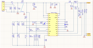
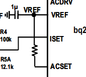
The following picture is the schematic diagram I designed for BQ24171. Could you please help review if it is correct? Thank you.

Among them, my power input specification is 5V output, single battery, battery voltage is 4.40V ± 0.05V, and charging current is 2A ± 0.1A.


At the same time, I would like to ask the following questions:

1、 According to the introduction of BQ24171 specification book, the pre charging current is 0.1 times the fast charging current, and the charging current drops to 0.5 times the charging current of 10-60 ℃ when Cold is between 0-10 ℃. These are fixed parameters. Is there any other way to reduce the pre charging current to 0.08A while ensuring a fast charging current of 2A, and the charging current of Cold is reduced to 0.8A when Cold is between 0-10 ℃? If there is any way, please share with me for reference.

2、 If my battery comes with a thermistor, can I directly pull the TS pin onto the battery, or should I keep the thermistor connected to the TS pin?

3、 Does BQ24171 have battery backflow protection?

4、 What is the function of the System? According to the schematic diagram below, the System is directly connected to the battery. Is this correct?

5、 Is the usage of D103 freewheeling diode in the following schematic correct? I am using a 1000V/2A fast tube

6、 When there is input, does the LED light keep flashing without connecting to the battery?

Thank you for the above. Looking forward to your reply


The schematic diagram is as follows

  • Hi dxd,

    On the schematic, if only powered by USB-C 5V, there is no need for the input snubber  .  Also, I question the sizing of the OVPSET resistors, which also sets UVLO.  I could not check the TS pin resistors since I don't know the details of the thermistor.  I recommend using the spreadsheet at the link below to double check. https://www.ti.com/lit/zip/sluc244

    Regarding 1, the only way to reduce precharge would be to change the ISET resistor divider.  You might be able to add a FET, with gate driven by battery voltage, and series resistor to change the bottom ISET resistor.

    Regarding 2, the battery thermistor should be connected to the TS pin.

    Regarding 3, no.  There is a path through the inductor, then high side internal FET body diode to PVCC.  So, I recommend adding a reverse blocking FET, driven by ACDRV, in order to prevent the battery voltage appearing at the USB-C + terminal.

    Regarding 4, yes.  If using the ACDRV FET and BATDRV FETs, the input source powers the system and charges the battery.  When the input source is removed, the BATDRV turns on the battery FET so that the battery can power the system.

    Regarding 5, there is an internal diode from REGN to BTST so D103 isn't needed.  We recommend a Schottky from SW to GND and this usually referred to as the freewheeling diode.

    Regarding 6, yes.  It is because of battery detection:

    I am puzzled why you using this device for a 5V input.  The BQ25616 is a better choice.

    Regards,

    Jeff

  • Hi  Jeff

    Nice to receive your reply

    I have revised the schematic again and marked the parameters based on your response. Could you help me confirm again

    Based on your response, I would like to ask you the following questions

    Question 1:Regarding modifying the pre charging current and the charging current at Cold 0-10 ℃ while ensuring a charging current of 2A. I roughly understand your suggestion. Could you please provide a complete solution

    Question 2:Can I understand that SYSTEM is connected to an external device? Is it possible for me to not use it in practical applications

    Question 3:Can we avoid the situation where battery free LED flashes? My client needs the LED light to not flash even without a battery

    Question 4:Why do you use BQ24171 for 5V input? It's because this is the IC specified by my customer.

                        At the same time, you said that using BQ25616 is better. Could you please tell me why it is more suitable compared to BQ24171

    Looking forward to your reply above

  • Hi dxd,

    Please refer to the detailed schematic checklist here

    Q1: You need a switch to change the resistance on the ISET. You need detection and control. 

    Q2: Yes

    Q3: No. The indication can't be changed.

    Q4: BQ25606 (if the VBAT needs to be 4.40V, please check Page 4 of BQ25616 DS) has fully integrated solutions including the reverse blocking FET, sensing and feedback networks, higher efficiency. The benefits for 5V input source charging using BQ256xx are lower BOM cost, better efficiency (for 1S only) and easy design, etc. The BQ25606 schematic checklist is here

    Regards,                                     

    Eric 

  • Hi ezhao

    I would like to consult you regarding the following issues during debugging

    According to the above image, charging needs to meet these conditions. During debugging, I tested that the ISET voltage was 0.4V, Vavcc voltage was 5V, OVPSET voltage was 1V, VREF was equal to 3.3V, and TS voltage was also within the allowable charging range.

    Q1:I'm not sure what this 1.5-s means?

    Q2: Is the voltage of REGN LDO 6V? What is the reason why the voltage I tested did not reach 6V?

    Q3:

    What are the differences in the connection methods between these two ACSETs? The second method is to directly connect a resistor to the ACSETs. What is the resistance value chosen for this resistor?

    Q4 :Because I didn't use SYSTEM, I don't need to consider ACFET, right?

    Q5:My PCB board has no output, but the LED is constantly on. After measuring the voltage of the protected PIN pin one by one, it is also within the specifications. Therefore, I think there should be no protection, but there is still no output. I would like to ask what the problem is

  • Hi Dxd,

    Regarding 1, 1.5 seconds.

    Regarding 2, the LDO linear regulator can only provide output voltage lower than the applied input voltage.  If you apply 5V, the LDO can't be 6V and will be running in drop out.

    Regarding 3, if not using input current limit, ACSET can be tied high.  If you using input current with a sense resistor between ACN and ACP, the resistor divider sets the max input current to the charger.

    Regarding 4, you do not need one of the 2 FETs but you will need at least a diode to block the battery voltage from appearing on the input.

    Regarding 5, your resistor divider on OVP SET also sets the undervoltage protection limit to 5.5V.  If you apply less than 5.5V input, the charger will not turn on.

    Regards,

    Jeff

  • Hi Jeff

    The input range set for my OVP is 2.5V to 8V, and my input is 5V, which should be sufficient. My problem is that the voltage of each setting pin is correct, but there is no output. I would like to ask what may be causing this problem

  • HI dxd,

    The OVPSET resistors in the schematic above don't give 2.5V to 8V.  Regardless, I don't understand why your LED is on, which is STAT low.  STAT low is charging:

    A fault cause STAT blinking.  Can you send an oscilloscope shot of PH, PVCC and SRN to confirm that the converter is switching?

    Regards,

    Jeff