This thread has been locked.

If you have a related question, please click the "Ask a related question" button in the top right corner. The newly created question will be automatically linked to this question.

LM51231-Q1: Supply is using "Lower VOUT Range" with 35K resistance between VREF and AGND when "Upper VOUT Range" should be used

Part Number: LM51231-Q1
Other Parts Discussed in Thread: LM5123EVM-BST,

Hello,, thanks for taking the time to look at this.  I've spent about a week trying to figure out this issue and could use some help.

I've designed a test board using the LM51231QRGRRQ1 which is based on the LM5123EVM-BST evaluation board.  The values on the schematic (attached) are the current values being tested.

The design is operating in FPWM mode with the expectation that it would output 24VDC.  It's on a 2-layer board that has not been optimized for EMI and we've already done a design review to tighten up ground loops and remove thermal relief on pads and vias.  The prototype is being tested with a 10 ohm resistive load.

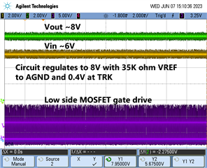
The VREF resistance to AGND is 35K ohm, the TRK voltage is set for 0.4V, and VREF is 1.0V.  The actual measured resistance with a HP34401A multimeter is 34.886K ohms.  TRK and VREF voltages were verified.  This should set the output voltage to 0.4V*60 = 24V.  However, the actual output is 8.0V indicating the "Lower VOUT Range" of 0.4V*20 (section 7.3.7 of the LM51231-Q1 October 2022 datasheet). 

The circuit goes into output bypass mode at 8.5V and operates normally at 8.0V, UVLO range is set between 6-7V.

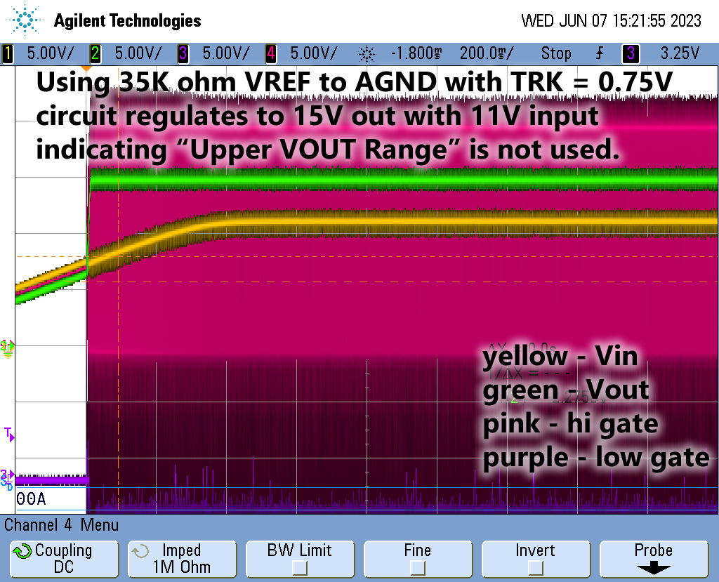
Changing the voltage divider from VREF to TRK to AGND to 6.8K and 21K sets the TRK voltage to 0.75V and the supply operates is enabled at 7V and has a regulated output of 15V (20*0.75).

It seems that regardless of the resistors used to set the output voltage the device is not using the "Upper VOUT Range".  This leads me to believe something is going wrong during Configuration Mode (datasheet 7.4.1.2), or the datasheet is wrong. 

I've done considerable testing including removing MOSFETS and inductor from the LM5123EVM-BST board and using them on my board.  I've added input and output capacitance, I've tested resistors that would enable the "Lower VOUT Range" to see if the datasheet resistor values were swapped.  The output regulated voltage is still TRK voltage*20.  


Here's what I found: 
1.  Using 35Kohm for VREF to AGND and 0.4V for TRK the circuit will not configure VOUT to be 0.4V*60.  With 16V supplied as the input voltage the circuit will begin active operation as the input exceeds UVLO at around 6V.  It will continue attempting to regulate the output to 8V (0.4*20, not 0.4*60) until the input supply reaches over voltage protection at about 8.5V and then enter FPWM bypass mode.  Shortly thereafter, as the input continues to rise the, the circuit turns off high and low MOSFETs and the output is VIN - MOSFET internal diode drop.

You would expect this operation if the resistance from VREF to AGND was 65Kohm (datasheet examples section 6.5).  But not if the resistance from VREF to AGND is 35K ohms.

2.  Changing the resistors from VREF to AGND to sum 30Kohm ensuring that the VREF to AGND resistors are not marginally outside the 35Kohm range in the datasheet has no impact.  Vout is still regulated to TRK voltage * 20 and not  TRK voltage * 60.

3.  Changing the input voltage to 11V and setting the TRK voltage to 0.75 with a total of 28K ohms between VREF and AGND results in the power supply regulating a VOUT of 15V from the VIN of 11V .  This again indicates that the IC is not using the "Upper VOUT Range" described in the datasheet.

Possible causes:
1.  Something on my test board is causing configuration mode to read the VREF to AGND resistance wrong and it's either reading the "Low VOUT Range" or just defaulting to it.

2.  The LM51231-Q1 datasheet is wrong, or incomplete and not indicating changes between the LM51231-Q1 and the LM5123.

3.  There's a functional difference between the LM51231-Q1 I'm using and the LM5123 on the evaluation board.  The evaluation design does regulate to 0.4*60 with 35K ohms between VREF and AGND.


VOUT Range".  +
Step-Up Supply r1_0.PDF


  • Hi Lon,

    Thanks for reaching out to us via e2e.

    It is a bank holiday today. Please expect a response by Friday or Monday.

    Best regards,

    Feng Ji

  • No problem.  Have a nice holiday.  I do think the issue is the configuration mode and my test board layout.

    I replaced the LM5123 with an LM51231-Q1 on the LM5123EVM-BST.  It correctly regulates the output voltage to 24V with an input voltage of 16V.  There doesn't appear to be any issue with the LM51231-Q1 datasheet or silicon differences between the LM51231-Q1 and LM5123.  So this should indicate that there is an issue with my test board not correctly detecting "Upper VOUT Range" during the configuration mode on power up.     

    Is there additional timing/information around configuration mode (datasheet section 7.4.1.2) other than the 120uS period  and VCC > Vvccc-uvlo?  My problem seems to be based on the test board incorrectly allowing detecting the resistance from VREF to AGND during power up.


  • Hello, 

    Thanks for reaching out. Does your board have a similar layout to the one of the EVM? We might share the EVM files in order to have a better comparison. Is there any other circuitry on your test board that might interfere with the LM5123(1-Q1) ? 

    Kind regards,
    EM

  • Hey EM, sorry for the late reply, I had a vacation last week.

    The test PCB was not laid out similar to the EVM.  It is a two layer board, I used thermal relief for pads and vias unlike the EVM, and there were some ground loops longer than necessary.  What didn't work is that the IC did not recognize the 35K ohm resistance on VREF and operate in the "Upper VOUT Range".  When I changed the TRK voltage to 0.75 with ~28K ohms from VREF to AGND the supply output 15V.  That would be the correct voltage for the "Lower VOUT Range".    

    This seems to indicate the Configuration Mode is not correctly measuring the resistance at VREF.

    There is no other circuitry on the board.  But this test PCB was just to validate the power supply, and the circuit will be added to a larger design with much more circuitry.

    I have re-designed the PCB to remove the thermal relief, and have less obstruction of the ground paths.  Attached is a PDF of the newer layout.
      6114.Step-Up Supply r1_0.PDF


  • Feng Ji,

    Can you provide any information on when the power supply IC enters and exits Configuration Mode after power is applied to the circuit.  

  • Hi Leon,

    Sorry for the late response. Please give us some time. We will be back with an answer until beginning of next week.

    Kind regards,

    Moritz

  • Hi Lon,

    I cannot imagine it has something to do with the timing of the configuration mode. It is possible that the IC is damaged, can you try to change it? Please check the soldering points at the TRK, AGND and VREF pin.

    Some points regarding the Layout:

    - The parts like R9, C24.. should be connected to the AGND plane.

    - PGND should be better connected, not only through the vias under the IC

    - The VCC capacitor should be better connected

    - in general we recommend to follow the layout guidelines that are provided in the datasheet

    We are looking forward for your response.

    Best regards,

    Moritz

  • Thanks for the response. 

    Before sending off the second version of the prototype board (the pdf you commented on) I did extend the AGND plane and connected R9, C24, and R4 to that top layer ground plane (that the compensation etc parts are connected to).  Unfortunately, I didn't improve the VCC capacitor location.  I'll have this board this week to see if the issue is still present.

    Can you expand on the better connection of PGND?  I made the connection based on the layout guidelines on page 34 of the datasheet.  Specifically "Connect power ground plane (the source connection of the QL) to EP through PGND. Connect the common analog ground plane to EP through AGND. PGND and AGND must be connected underneath the device."  I can see that the bottom layer traces could impact PGND connections. 

    For the original test board I did build two, and both had the "lower VOUT range" issue.  I also replaced the LM5123 on the EVM with an LM51231 to verify no differences between the older and newer parts.  After replacement the EVM continued to operate using the "upper VOUT range" correctly.  I also replaced the ICs on my boards to ensure the LM51231 wasn't damaged.

    One concern I had was that in the hand-built prototypes solder flux could be contributing additional resistance causing a measurement error in configuration mode.  But DMM measurements didn't show that, and replacing the IC on the EVM didn't result in the problem existing in the EVM (I used the same flux).

    In the final design, which will be machine assembled, I can move parts closer to the IC, and although not preferred a 4-layer board is an option.          
     

  • Hi Lon,

    Thanks for your reply. Please try to connect the UVLO directly to Vin. Without any other connection.

    Kind regards,

    Moritz

  • The newest prototype board is operating in the "Upper VOUT range" with a voltage output of 24VDC and an input of 16.5VDC.  So it looks like the issue was related to board layout, probably grounding, in the first attempt.